Purpose:
- Converting alternating current into unidirectional pulsating current (current rectification).
- Isolation of average rectified and rms current values (diode detectors).
- Protection of devices from incorrect switching polarity, protection of circuit inputs from overload, switches from breakdown of self-induction emf that occurs when an inductive load is turned off, etc.
- Switching high frequency signals.
- Limiting or stabilizing the voltage level.
- Detecting the presence and level of illumination.
- Emission of light.
Diode classification:
By installation method:
- for surface mounting (SMD/SMT);
- for surface mounting (TH);
- integral (thin film).
By purpose:
- Rectifiers;
- Pulse;
They have a short duration of transient processes and are intended for use in pulsed operating modes.
- Detector;
- Mixing;
Designed to convert high-frequency signals into signals of a difference frequency determined by the frequency of the master oscillator.
- Switchable;
Used in microwave power level control devices.
- Restrictive;
- Protective;
Protection of equipment from increased mains voltage.
- Generating;
Used to generate HF and microwave oscillations.
- Reception;
- Radiative.
By design:
- Schottky diode;
- Microwave diode;
- Zener diode (Zener diode);
- Varicap;
- Light-emitting diode;
- Photodiode;
- Pin diode;
- Avalanche diode;
- Avalanche diode;
- Gunn diode;
- Tunnel diode;
- Reversed diode.
By p-n junction size:
- planar;
- point.
By frequency range:
- Low frequency;
- High frequency;
- Microwave.
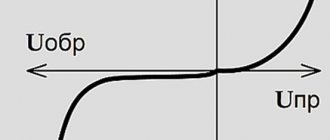
I-V characteristic of the diode:
First, let's look at the current-voltage characteristic of an ideal diode.
Figure 1 - I-V characteristic of an ideal diode.
As can be seen from the graph, the diode conducts current only when there is a forward voltage at its terminals (i.e., plus at the anode, minus at the cathode). Current I 0 is the saturation current, i.e. The maximum reverse current caused by the thermal drift of current carriers in the region of the pn junction is several orders of magnitude less than the forward current.
For fans of formulas, it can be noted that the current-voltage characteristic of an ideal diode is described by the following expression:
Spoiler
Where:
I 0 – saturation current.
— thermal potential (e is the elementary charge of the electron, k is Boltzmann’s constant, T is the absolute temperature).
However, in life, as you know, not everything is so simple and you have to constantly strain your brain. The current-voltage characteristic of a real diode is somewhat different.
Figure 2 - I-V characteristic of a real diode.
The first difference is the different diode opening voltage ( U0 ), depending on the semiconductor material used . For silicon ( Si ) it is approximately 0.7 V ; for germanium ( Ge ) – 0.3 V.
The second difference is a different type of reverse branch, the presence of a breakdown of the pn junction.
Usually, areas of electrical (A-B) and thermal (B-C) breakdown are distinguished. Electrical breakdown inherently violates only the electrical insulation of pn junction regions, so it is reversible. Thermal breakdown, on the contrary, violates the physical integrity of the pn junction; in fact, it simply burns out; it is obvious that thermal breakdown is irreversible and renders the element unusable.
If you are interested in the reasons for the breakdown, then the next paragraph is for you.
Spoiler
Main characteristics and parameters of diodes
I-V characteristics of the diode
For the device to work correctly, it must be selected in accordance with:
- Current-voltage characteristic;
- Maximum permissible constant reverse voltage;
- Maximum permissible pulse reverse voltage;
- Maximum permissible direct direct current;
- Maximum permissible pulsed direct current;
- Rated direct direct current;
- Direct direct voltage at rated current;
- Constant reverse current, indicated at the maximum permissible reverse voltage;
- Operating frequency range;
- Capacity;
- Breakdown voltage (for protective diodes and zener diodes);
- Thermal resistance of the housing for various installation options;
- Maximum permissible power dissipation.
Electrical breakdown:
Electrical breakdown occurs due to a sharp increase in reverse current due to a sharp decrease in the resistance of the barrier layer.
An attentive reader will immediately object: “how can this be? After all, an increase in the reverse voltage for a pn junction causes an increase in the geometric dimensions of the blocking layer, and, consequently, its resistance!” And this matter is explained quite simply. Reality always comes up with some difficulties for us, so in semiconductors there are two phenomena - avalanche charge multiplication and the tunnel effect, by name, which divide electrical breakdown into avalanche and tunnel. And if to understand the first effect it is enough to read about its essence, then the tunnel effect is a quantum effect, and to understand it you simply need to strain your brain. Avalanche charge multiplication occurs due to the phenomenon of impact ionization, the essence of which is that electrons, accelerated by an electric field, acquire energy sufficient to knock electrons out of the atoms of the semiconductor crystal lattice, which in turn are also accelerated by this field, and the so-called “avalanche” process of electron separation from atoms by an electric field. The result of these processes is a sharp increase in conductivity, and, consequently, a decrease in the resistance of the barrier layer with virtually no change in its geometric dimensions.
The tunnel effect (also known as the Zener effect in English literature) is most likely in pn junctions of small thickness. Its essence is that electrons having a total energy less than the height of the energy barrier still penetrate through this energy barrier, in our case the barrier of the pn junction, without changing energy, at such voltages when the conduction band in the n-region has equal energy levels with a p-region valence band. This effect is completely quantum and contradicts classical mechanics. As a simplified explanation, we can say the following. From the solution of the Schrödinger equation for the problem of a potential barrier, it follows that the barrier transparency coefficient is non-zero for particles with an energy equal to or less than the height of this barrier. Well, in order to eliminate possible logical difficulties, we can recall the uncertainty relation (Heisenberg relation), which says that if we reduce the uncertainty in the coordinate of a particle, then we increase the uncertainty in the momentum, and vice versa. Consequently, We cannot say with certainty that the particle that passed the barrier actually had a certain energy at the moment of passage.
It should also be noted that the tunnel effect is probabilistic in nature, so the highest probability of its occurrence is in pn junctions with a high concentration of impurities.
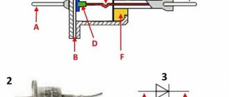
Gunn diode
The Gunn diode consists solely of an N-type semiconductor. Thus, it is not a true diode. The figure below shows a lightly doped N– layer surrounded by heavily doped N+ layers. A voltage applied to an N-type gallium arsenide Gunn diode creates a strong electric field in the lightly doped N– layer.
Gunn Diode: Oscillator circuit and diode cross section of N-type semiconductor only.
As the voltage increases, conductivity increases due to electrons in the low-energy conduction band. When the voltage exceeds a threshold of approximately 1 V, electrons will begin to move from the lower conduction band to the higher energy conduction band, where they no longer contribute to conduction. In other words, as the voltage increases, the current decreases, the phenomenon of negative resistance. The oscillation frequency is determined by the transit time of conduction electrons, which is inversely related to the thickness of the N– layer.
The frequency can be controlled to some extent by placing a Gunn diode in the resonant circuit. The equivalent circuit shown in the figure above is actually a coaxial transmission line or waveguide. Gallium arsenide Gunn diodes are capable of operating in the range from 10 to 200 GHz at powers from 5 to 65 mW. Gunn diodes can also serve as amplifiers.
Parasitic properties of the diode:
Temperature influence:
Since drift processes in a semiconductor play an important role, temperature can significantly change the current-voltage characteristics of the pn junction and, accordingly, the parameters of the diode.
Figure 3 - Effect of temperature on the diode's current-voltage characteristic.
Where:
— normal ambient temperature ();
— operating temperature of the diode.
Diode characteristics
History of the diode
The appearance of the diode is due to the British scientist Frederick Guthrie and the German physicist Karl Ferdinand Braun.
In 1873 and 1874, they discovered the working principle of thermionic diodes and the working principle of crystal diodes. Later, specialized vacuum tubes began to be called thermionic diodes. In early 1880, Thomas Edison re-documented the operation of the thermionic diode, but the development of this radio-electronic component did not occur until 9 years later, when the German scientist Karl Braun demonstrated the operation of an on-chip rectifier. At the beginning of the 20th century, Greenleaf Picard presented to the public the first radio receiver, which was based on the properties of a diode to respond to electromagnetic vibrations. Industrial production of thermion-type diodes (lamp diodes) was established in Britain with the permission of John Fleming in 1904, and 2 years later the American Picard patented the first detector made of silicon crystals. The modern terminology of the word “diode” (from the Greek “di” - two, “odos” - path) was introduced by William Henry Ickles in 1919. In the USSR, the main role in the development of semiconductor components was played by physicist B. M. Vul. The first development was achieved by tube diodes or kenotrons (electric vacuum diodes), as well as gas-filled diodes (gastrons, zener diodes, ignitrons). However, the main contribution to the development of radio-electronic components was made by semiconductor diodes based on silicon and germanium.
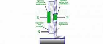
Physical basis of diode operation
The chemical element “germanium” was discovered in 1882 by Clemens Winkler in the process of studying electricity and made it possible to identify the effect of a current semiconductor. Experiments by physicists to obtain a one-way current conductor have led to the result that if an acceptor impurity (barium, aluminum, gallium or indium) capable of capturing electrons accumulated in germanium is added to germanium, the result will be an electronic element capable of passing electrons into only one side (from germanium to the acceptor mixture). As we know, an electron is a negatively charged particle that is attracted to a positive particle, but in electronics the designation for the movement of current from plus to minus is accepted. Thus, the diode is a mixture of germanium or silicon with an acceptor material. Germanium, due to the accumulated electrons, carries a negative N charge (N - negative), and the acceptor mixture is saturated with positive P ions (P - positive). The process of current flowing from the P region to the N region through the “junction” or pn junction is the principle of operation of the diode. Its feature is that current can flow only in one direction, so the diode is a unidirectional semiconductor. The negatively charged side with germanium is usually called the “cathode”, and the positively charged half the “anode”. In diagrams, a diode is indicated by the direction of current flow in the form of an arrow towards the negatively charged side.
When the diode is not connected to a power source, the pn junction is at rest. And as a result of the attraction of electrons to positive ions, they drift through the junction. This process is called “diffusion,” which involves the attraction of electrons through the transition to the “holes” of positive ions. Diffusion movement due to the constantly changing concentration of ions and electrons occurs near the junction constantly.
When an external voltage source or bias voltage is connected to the pn structure, the conditions for charge transfer through the junction change. An important factor here is the polarity of the external voltage connected to the anode and cathode of the diode.
Direct voltage connection to pn structure
When the diode is connected directly, when the plus of the power source is connected to the p-region, and the minus to the n-region, current flows directly through the junction. In this case, electrons located in the n-region, due to the connected minus of the power source, will move closer to the junction. Actually, the same effect will occur with positively charged particles in the p-region. As a result, the pn junction will be filled with electrons in the “holes” (positive ions). An electric field will arise that will allow free electrons to overcome the junction resistance, pass through the barrier zone and p-region to the positive contact of the power source. An electric current will arise in this circuit, which is called the forward bias current of the junction. The magnitude of this current will be limited by the technical characteristics of the diode.
The moment when an electric field is created in the pn junction on the positive branch of the Volt - Ampere Characteristics of the diode (VC) is marked by a certain voltage ∆Ua. This voltage is determined not only by the current strength, but also by the resistance of the pn junction itself. The lower this resistance, the less energy is needed to open the transition, as well as close it. Digression from the topic of the article, it is worth saying that the energy in the transition does not immediately disappear when the power supply disappears. A charge resorption effect occurs due to the junction capacitance. The lower this capacitance, the faster the diode will go into the “off” state, calming down all transient processes in the pn junction. This parameter is very important in frequency diodes, which we will discuss below. In modern diodes, voltage values ∆Ua vary from 0.3 to 1.2 volts (silicon 0.8 - 1.2 V, germanium 0.3 - 0.6 V) depending on the power of the diode. It is also called pn junction voltage drop.
Reverse voltage connection to pn structure
When connected to a power diode in the reverse direction, the resistance of the pn junction increases and the barrier increases, due to the fact that it is easier for electrons in the n-region and free ions in the p-region to connect with the charge of the power source. As the supply voltage increases, an avalanche-like outflow of charged particles from the junction occurs. As a result, the diode goes into the off state due to reverse voltage.
On the reverse branch of the current-voltage characteristic, the 0 – 1 section is caused by a small reverse voltage. In this case, an increase in the reverse current is observed due to a decrease in the diffusion component. In other words, minority carriers are present in the p and n regions. Even when the diode is closed, they can flow through the barrier at low voltage from one area to another. The value of this current is disproportionately small compared to the direct current, since the number of minority carriers in different regions p and n is minimal. Starting from point 1, the majority carriers are no longer able to overcome the barrier, and the diffusion minority carriers are completely absorbed into their transition regions. This explains the lack of current growth with increasing reverse voltage. Since the concentration of minority charge carriers depends on the temperature of the alloy (aka “crystal”), the reverse current will increase as the temperature of the crystal increases. That is why it is called thermal. This is an avalanche-like process and it obeys the exponential law. It is because of the reverse currents that the diodes begin to heat up and are installed on heat sinks. If the reverse current value is higher than that provided by the diode, then an uncontrolled process of so-called thermal breakdown will begin, followed by an electrical breakdown, rendering the diode unusable. Stable operation of silicon diodes is possible at temperatures of 130 – 135 degrees. The destruction of the crystal of germanium diodes occurs at a temperature of 50 - 60 degrees.
Full volt-ampere characteristic of the diode
The volt-ampere characteristic displays the dependence of the current flowing through the diode on the magnitude of the applied forward and reverse voltage. The steeper and closer to the Y axis the forward branch and the closer to the X axis its reverse branch, the better the rectifying properties of the diode.
When the reverse voltage is disproportionately large, the diode experiences an electrical breakdown. In this case, the reverse current increases sharply. Normal operation of the diode is possible if the reverse voltage applied to it does not exceed the maximum permissible, called breakdown voltage. As we have already written, diode currents depend on the temperature of the crystal. For every degree the voltage drop across the pn junction changes by 2mV. If the temperature of the crystal increases upward, then the reverse current of germanium diodes increases by 2 times; for silicon diodes, the reverse current increases by 2.5 times for every 10 degrees. In this case, the breakdown voltage decreases with increasing temperature.
Diode design
According to their technological design, diodes can be planar or point diodes. The Pn junction of planar diodes (in Figure b - a planar alloy diode) is performed at the boundary of two layers in a semiconductor. The layers have different types of electrical conductivity. Due to the larger junction area, planar diodes can pass large currents through themselves. Their disadvantage is a large transition capacitance, which limits the use of planar diodes in high-frequency technology. However, there are hybrid diodes that combine low capacitance, low contact resistance, and the ability to pass high currents. An example would be the domestic diode KD213.
For point diodes, the pn junction is made at the point of contact of the semiconductor wafer with the tip of a metal needle. Modern diodes are produced using germanium, silicon, gallium phosphide and gallium arsenide.
Types and characteristics of diodes
Rectifier diodes
Rectifier diodes are used to rectify alternating currents at frequencies typically below 50 kHz. The design of such diodes is predominantly planar. Due to this, diodes allow large rectified currents to pass through themselves. For the most part, the material used to manufacture rectifier diodes is silicon due to its resistance to temperature changes. The main parameters that determine the characteristics of the diode are:
Upr. – constant forward voltage on the diode at a given constant forward current.
Urev. – constant voltage applied to the diode in the opposite direction.
Ipr. – direct current flowing through the diode when connected in the forward direction.
Iobr. – direct current flowing through a diode connected in the reverse direction.
Ipr.av. – direct current averaged over the period.
Irev.av. – reverse current averaged over the period.
Rdif. – the ratio of the voltage increment on the diode to the small current increment that caused it.
In addition, of all types, there are BASIC CHARACTERISTICS OF DIODES, which determine their maximum technical capabilities, which include:
Urev.max – maximum voltage applied when the diode is turned back on.
Ipr.max – maximum permissible direct direct current (one of the most important parameters).
Ipr.av.max – maximum permissible average forward current.
Ivp.av.max – maximum permissible average rectified current.
Additional parameters include the operating temperature range.
Rectifier diodes are widely used in electronic circuitry. Based on them, you can often find diode bridges for changing the shape of the current from alternating to direct.
Modern development of electronics is impossible without the use of high-frequency diodes.
High frequency diodes
These diodes are used in a wide range of frequencies up to several hundred megahertz and above. Most often they are used for modulation and detection, as well as in high-frequency radio circuits. As high-frequency diodes, elements made in a point design are used due to the low junction capacitance.
For such diodes, two additional characteristics are important: the maximum operating frequency in MHz and the diode capacitance in pF.
Pulse diodes
Pulse diodes are designed to convert pulse signals. In power circuitry, high-power pulse diodes can work as rectifiers. An example is a switching power supply, where they are used in the secondary circuit after a pulse transformer. Pulse diodes are also used in television equipment (video signal detectors), in key and logic devices. There are two and three electrode pulse diodes (paired). Three-electrode diodes can be with a common anode or a common cathode. Pulse diodes have the following additional characteristics:
Upr.i – peak forward voltage at a given current pulse.
Urev.i – accordingly, the reverse voltage at the peak is both single and periodically repeating.
CD is the total capacitance of the diode at given voltages and frequencies. A large parameter CD reduces the frequency properties of the diode. The following parameter also directly depends on the value of SD.
τres – recovery time from the end of the current pulse to the state of a given reverse blocking voltage (end of transient processes of charge resorption in the pn junction)
Qpc is part of the accumulated charge flowing into the external circuit when the current reverses from the direct value to the reverse.
One of the main parameters of Schottky diodes is
Ipr.i max – maximum permissible PULSE direct current.
Zener diodes and stabilizers
This type of diode is necessary in voltage stabilization circuits when the current passing through the diode changes. Its main characteristics are:
Ust - stabilization voltage.
Ist. max and Ist. min – maximum and minimum stabilization current.
Pmax – maximum permissible power dissipation.
For zener diodes, the working part is the breakdown section of the current-voltage characteristic. In the figure it is marked by the distance between the points Ist.min and Ist.max. In this section, the voltage on the zener diode remains constant even with a significant change in the current value. For stabistors, the working part is the direct section of the current-voltage characteristic. There are also dual-anode zener diodes, which include two back-to-back pn junctions. Each of these transitions is the main one when changing the polarity of its connection.
Varicap
Special semiconductor diode. Its pn junction capacitance varies significantly depending on the reverse voltage applied to it. If the reverse voltage increases, the junction capacitance decreases and vice versa. Varicaps are actively used in local oscillators (radio units where frequency adjustment is necessary). For example, varicap can often be found in FM radio receivers. The main characteristics of a varicap include:
CH – measured capacitance at a given voltage.
Kc is the ratio of capacitances at the minimum and maximum permissible voltage.
Irev – maximum current flowing through the varicap in the reverse direction. (leakage current).
Tunnel diode
The tunnel diode is used in high-frequency amplifiers and electrical oscillators (for example, television amplifiers). In addition, it is used in various pulse devices. Its feature is the A-B section with a negative differential resistance, which determines the ratio between the change in voltage and the increase in current. Its additional parameters include:
Iп – direct current at the maximum point of the current-voltage characteristic, at which the increment of current to voltage is equal to 0.
Ld is the inductance of the diode, which prevents the passage of a high-frequency signal.
Ksh is the noise component of the diode.
Rп – loss resistance of the tunnel diode.
Schottky diode
A popular diode in radio engineering due to its low noise and high performance. It is classified as a subtype of pulse diodes. Technologically, the Schottky diode is made of a metal-semiconductor structure. The use of Schottky barrier diodes is very diverse, from ATX PC power supplies to microwave devices. The Schottky diode junction is made according to the pin principle, where i is a high-resistance lightly doped semiconductor. Under the influence of voltage, its frequency characteristics change, which allows the diode to be used in signal control circuits, for example, attenuators, level limiters, modulators. Powerful Schottky diodes can be used as rectifying radioelements of frequency power supplies.
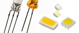
Light-emitting diode
A special type of diode that can produce non-cogenerative radiation (the emission of visible photons of light from pn junction atoms). Depending on the amount of doping material, the length of the spectrum is changed. Due to this, LEDs can be produced in different colors. LEDs are widely used: from warning signal circuits to household lighting. In addition, when using special manufacturing materials, the LED can emit in the infrared spectrum. This property has found application in remote controls and other electronic devices. Modern LEDs are made at high powers (up to 10 W). The pn junction is very sensitive to current changes, so to use it you need a specialized driver, which is a current stabilizer / regulator.
Photodiode
Often used to receive infrared light spectrum, as well as in galvanic isolation circuits. In addition, the first solar cells used a photodiode. Together with emitting diodes or transistors, it can form a single device called an optocoupler. The operation of a photodiode is based on the photovoltaic effect, in which an emf begins to appear due to the separation of electrons and holes in the pn junction. Depending on the degree of illumination, the level of the generated EMF in the photodiode also changes.