Semiconductor materials.
Also on topic:
ELECTRONICS INDUSTRY
A semiconductor is a material that conducts electricity better than a dielectric such as rubber, but not as well as a good conductor such as copper. Unlike metals, the electrical conductivity of semiconductors increases with increasing temperature. The best semiconductor materials include silicon (Si) and germanium (Ge); others include compounds of gallium (Ga), arsenic (As), phosphorus (P) and indium (In). Silicon has many uses in transistors, rectifiers and integrated circuits. Gallium arsenide (GaAs) is commonly used in microwave and optoelectronic devices, as well as integrated circuits. see also
PERIODIC SYSTEM OF ELEMENTS; INTEGRATED CIRCUIT; SOLID STATE PHYSICS; TRANSISTOR.
A semiconductor is essentially a dielectric until a small and carefully measured amount of some suitable material is introduced into it. For example, a material such as phosphorus makes silicon conductive by adding excess electrons to it (i.e., acting as a “donor”). Silicon doped in this way becomes silicon n
-type.
Doping with a material such as boron transforms silicon into a p
-type material: boron (the acceptor) takes away some of the electrons from the silicon, creating “holes” in it, which can be filled with electrons from nearby atoms and thereby increase the conductivity of the doped material. (The flow of electrons in one direction and holes in the opposite direction forms a current.) The electrons and holes that thus provide conductivity are called charge carriers.
SEMICONDUCTOR DEVICES
SEMICONDUCTOR DEVICES, electronic devices whose operation is based on electronic processes in semiconductors. In electronics, P.P. are used in devices for processing electrical power. signals, as well as for converting one type of energy into another. P. p. are divided into two large classes: discrete P. p., structurally designed in the form of a department. self-sufficient devices, and integrated P. p. - active elements of integrated circuits (primarily field-effect transistors with a metal-oxide-semiconductor structure, or MOS transistors, and bipolar transistors).
Discrete P. items are distinguished by purpose, principle of operation, type of base. PP material, design and technology, type of characteristics, areas of application. To the main Classes of such power supplies include: electrical converting devices used to convert electrical power. signals (semiconductor diodes, including varicaps, zener diodes, Schottky diodes; transistors, thyristors, etc.); optoelectronic devices that convert light signals into electrical signals and vice versa (photoresistors, photodiodes, phototransistors, photothyristors, solar cells, semiconductor lasers, light-emitting diodes, charge-coupled devices); semiconductor microwave devices (Gunn diodes, tunnel diodes, avalanche diodes, etc.); semiconductor nuclear radiation detectors; thermoelectric devices that convert thermal energy into electrical energy and vice versa (thermoelement, thermoelectric generator, thermistor, etc.); magnetoelectric devices (eg, Hall transducers); strain gauge devices that change their electrical resistance due to deformation caused by mechanical forces applied to it. stress, etc.
Depending on the semiconductor material used, germanium, silicon, gallium arsenide and other devices are distinguished.
In terms of design and technology. P.'s signs are divided into point and planar; the latter, in turn, are divided into alloy, diffusion, mesaplanar, planar, epiplanar, etc. The technology of most PPs is based on such fundamentals. processes such as protecting the PP surface with a thin film of dielectric, photolithography, diffusion of impurities and ion doping, deposition of thin films. P.p. are produced in metal-ceramic. or plastic cases that protect devices from external influences (with the exception of open-frame PP devices).
Small overall dimensions, weight and power consumption, high reliability and mechanical properties. strength contributed to the spread of power supplies and the rapid development of semiconductor electronics. To the beginning 2010s the nomenclature of P. items produced by industry in all countries of the world totaled St. 100 thousand types of various devices. applications operating both at the lowest frequencies (of the order of fractions of Hz) and in the millimeter range (up to several THz or more), in the operating power range from μW to several kW.
pn-Transitions.
Solid-state electronic devices are usually a multilayer structure (sandwich), one part of which is made of semiconductor p
-type, and the other is from an
n
-type semiconductor.
The boundary region between p
-type and
n
-type materials is called
p-n
junction.
The transition is formed by positively charged atoms of the donor impurity on the n
side and negatively charged atoms of the acceptor impurity on
the p
side.
The electric field created by these ions prevents the diffusion of electrons into the p
region and holes into
the n
region (Fig. 1).
If p
p-n
region is connected to the positive terminal of a voltage source (for example, a battery), and the
n
region is connected to the negative terminal, then electrons and holes can diffuse through the junction.
As a result, a significant current will flow from the p
-region in the direction of
the n
-region.
In this case, the transition is said to be forward biased. In reverse bias, when the connections described above are of opposite polarity, only a very small amount of reverse current will flow from the n
-type region to the
p
-type region.
PN Junction Diodes.
Diodes are devices that conduct electrical current in only one direction. Therefore pn
-transitions are ideal for use in diode rectifiers that convert alternating current to direct current.
When the reverse bias voltage on a pn
-transition increases to a critical value, called the breakdown voltage, the electric field in the transition region creates electrons and holes as a result of collisions of high-energy charge carriers with semiconductor atoms. During this process, called ionization, an “avalanche” of new carriers is formed, as a result of which the reverse current at the breakdown voltage increases significantly.
Diode rectifiers typically operate at reverse voltages below the breakdown voltage. However, the sharp and significant increase in reverse current that occurs when the breakdown voltage is reached can be used to stabilize the voltage or to fix the reference voltage level. Diodes designed for such applications are called semiconductor zener diodes. see also
ELECTRONIC CIRCUITS.
Capacitance depending on the applied voltage corresponds to the reverse biased pn
- transition. Such voltage-controlled capacitance can be used, for example, in tunable circuits. Diodes that use such junctions are called varicaps.
Sharp pn
-junctions, which have a very small thickness and are heavily doped on both sides, are used in tunnel diodes, i.e.
diodes, in which electrons can “tunnel” through a junction. Tunneling is a quantum mechanical process that allows some electrons to pass through a potential barrier. In both reverse and forward bias, a tunnel diode passes current at a very low voltage. But at a certain critical value of the forward bias voltage, the tunneling effect decreases, and, ultimately, the forward current from the p
-region to
the n
-region becomes predominant. The current due to tunneling continues to decrease as the voltage rises from a critical level to some higher value. In this voltage range, where tunneling decreases, negative resistance occurs, which can be used in various types of switches, oscillators, amplifiers and other electronic devices.
pn
-The junction can also find application as a photodiode or solar cell (photovoltaic junction).
When light, which consists of photons, illuminates a pn
junction, the atoms of the semiconductor absorb the photons, resulting in the formation of additional pairs of electrons and holes.
Because these extra carriers collect in the junction region, excess current flows from the n
-region to
the p
-region. The magnitude of this reverse current is proportional to the rate at which additional carriers are generated, and this rate in turn depends on the intensity of the incident light.
In photodiodes, this reverse current at a fixed reverse bias voltage depends on the illumination intensity. Therefore, photodiodes are often used in photometers and character recognition systems.
Received from pn
-transition energy is transferred by the solar cells to the external load connected to them.
Solar cells, which convert sunlight into electricity, are widely used as power sources for artificial Earth satellites and in some applications on Earth. See also
BATTERIES.
In many semiconductor materials, such as gallium arsenide (GaAs), gallium phosphide (GaP), and indium phosphide (InP), electrons and holes recombine with each other in the pn
-a junction shifted in the forward direction, emitting light.
The wavelength of the radiation depends on the material used; Typically, the emission spectrum ranges from infrared (as in the case of GaAs) to green (as for GaP) regions. With proper selection of materials, light-emitting diodes (LEDs) can be manufactured that will emit radiation of almost any color (wavelength). Such LEDs are used in digital wristwatches and in indicators of electronic calculators. Infrared LEDs can be used in optical communication systems, in which light signals sent through fiber optic cables are detected by photodiodes. Optoelectronic systems of this kind can be very effective if laser-type LEDs are used and photodetectors operate in avalanche mode with reverse bias. See also
FIBER OPTICS; LASER.
Semiconductors. Semiconductor devices
Brass Read more: Semiconductor diodes
2. Semiconductors. Semiconductor devices
2.1. General information
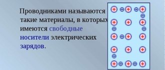
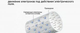
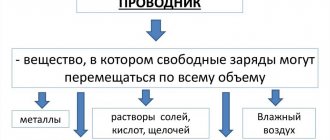
Semiconductors are substances whose conductivity is intermediate between the conductivities of metals and dielectrics. Semiconductors are both poor conductors and poor dielectrics. The boundary between semiconductors and dielectrics is arbitrary, since dielectrics at high temperatures can behave like semiconductors, and pure semiconductors at low temperatures behave like dielectrics. In metals, the electron concentration is practically independent of temperature, and in semiconductors, charge carriers appear only when the temperature increases or when energy is absorbed from another source.
Typical semiconductors are carbon (C), germanium (Ge), and silicon (Si). Germanium is a brittle, grayish-white element discovered in 1886. The source of powdered germanium dioxide, from which solid pure germanium is obtained, is the ash of certain types of coal.
Silicon was discovered in 1823. It is widely distributed in the earth's crust in the form of silica (silicon dioxide), silicates and aluminosilicates. Sand, quartz, agate and flint are rich in silicon dioxide. Pure silicon is obtained from silicon dioxide chemically. Silicon is the most widely used semiconductor material.
Let us consider in more detail the formation of conduction electrons in semiconductors using silicon as an example. The silicon atom has the serial number Z=14 in the periodic table of D.I. Mendeleev. Therefore, its atom contains 14 electrons. However, only 4 of them are on the unfilled outer shell and are weakly bound. These electrons are called valence electrons and give rise to the four valences of silicon. Silicon atoms are able to combine their valence electrons with other silicon atoms using what is called a covalent bond (Figure 2.1). In covalent bonding, valence electrons are shared between different atoms, resulting in the formation of a crystal.
As the temperature of the crystal increases, thermal vibrations of the lattice lead to the breaking of some valence bonds. As a result, some of the electrons that previously participated in the formation of valence bonds are split off and become conduction electrons. In the presence of an electric field, they move against the field and form an electric current.
Rice. 2.1
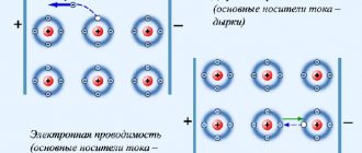
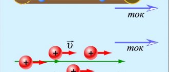
However, when an electron is released in the crystal lattice, an unfilled interatomic bond is formed. Such “empty” spaces with missing bonding electrons are called “holes.” The appearance of holes in a semiconductor crystal creates an additional opportunity for charge transfer. Indeed, the hole can be filled by an electron transferred under the influence of thermal vibrations from a neighboring atom. As a result, normal communication will be restored in this place, but a hole will appear in another place. Any of the other bond electrons, etc., can in turn go into this new hole. The sequential filling of a free bond with electrons is equivalent to the movement of a hole in the direction opposite to the movement of electrons. Thus, if in the presence of an electric field electrons move against the field, then holes will move in the direction of the field, i.e. the way positive charges would move. Consequently, in a semiconductor there are two types of current carriers - electrons and holes, and the total conductivity of the semiconductor is the sum of electronic conductivity (n-type, from the word negative) and hole conductivity (p-type, from the word positive).
Along with transitions of electrons from a bound state to a free state, there are reverse transitions in which a conduction electron is captured in one of the vacant positions of bond electrons. This process is called electron-hole recombination. In a state of equilibrium, such a concentration of electrons (and an equal concentration of holes) is established at which the number of direct and reverse transitions per unit time is the same.
The considered conduction process in pure semiconductors is called intrinsic conductivity. Intrinsic conductivity increases rapidly with increasing temperature, and this is a significant difference between semiconductors and metals, whose conductivity decreases with increasing temperature. All semiconductor materials have a negative temperature coefficient of resistance.
Pure semiconductors are an object of mainly theoretical interest. Major semiconductor research concerns the effects of adding impurities to pure materials. Without these impurities, most semiconductor devices would not exist.
Pure semiconductor materials such as germanium and silicon contain small numbers of electron-hole pairs at room temperature and can therefore conduct very little current. Alloying is used to increase the conductivity of pure materials.
Doping is the addition of impurities to semiconductor materials. Two types of impurities are used. Impurities of the first type - pentavalent - consist of atoms with five valence electrons, for example, arsenic and antimony. The second type of impurity - trivalent - consists of atoms with three valence electrons, for example, indium and gallium.
Rice. 2.2
When a pure semiconductor material is doped with a pentavalent material such as arsenic (As), some of the semiconductor atoms are replaced by arsenic atoms (Figure 2.2). The arsenic atom introduces four of its valence electrons into covalent bonds with neighboring atoms. Its fifth electron is weakly bound to the nucleus and can easily become free. The arsenic atom is called a donor atom because it donates its extra electron. The doped semiconductor material contains a sufficient number of donor atoms, and therefore free electrons, to maintain the current.
At room temperature, the number of additional free electrons exceeds the number of electron-hole pairs. This means that the material has more electrons than holes. Therefore, electrons are called majority carriers. Holes are called minority carriers. Since majority carriers have a negative charge, such a material is called an n-type semiconductor.
When a semiconductor material is doped with trivalent atoms, such as indium (In) atoms, these atoms will place their three valence electrons among three neighboring atoms (Figure 2.3). This will create a hole in the covalent bond.
The presence of additional holes will allow electrons to easily drift from one covalent bond to another. Since holes easily accept electrons, atoms that introduce additional holes into a semiconductor are called acceptor atoms.
Rice. 2.3
Under normal conditions, the number of holes in such a material significantly exceeds the number of electrons. Therefore, holes are the majority carriers and electrons are minority carriers. Because the majority carriers have a positive charge, the material is called a p-type semiconductor.
N- and p-type semiconductor materials have significantly higher conductivity than pure semiconductors. This conductivity can be increased or decreased by changing the amount of impurities. The more heavily doped a semiconductor material is, the lower its electrical resistance.
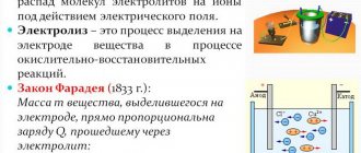
The contact of two semiconductors with different types of conductivity is called a pn junction and has a very important property - its resistance depends on the direction of the current. Note that such a contact cannot be achieved by pressing two semiconductors against each other. A pn junction is created in one semiconductor wafer by forming regions with different types of conductivity in it. Methods for obtaining pn junctions are described below.
So, in a piece of a single-crystal semiconductor, a pn junction is formed at the boundary between two layers with different conductivities. There is a significant difference in the concentrations of charge carriers. The concentration of electrons in the n-region is many times greater than their concentration in the p-region. As a result, electrons diffuse into the region of their low concentration (in the p-region). Here they recombine with holes and in this way create a spatial negative charge of the ionized acceptor atoms, which is not compensated by the positive charge of the holes.
At the same time, diffusion of holes into the n-region occurs. Here, a spatial positive charge of the donor ions, which is not compensated by the electron charge, is created. Thus, a double layer of space charge is created at the boundary (Fig. 2.4), depleted of the main current carriers. A contact electric field Ek arises in this layer, preventing the further transition of electrons and holes from one region to another.
The contact field maintains a state of equilibrium at a certain level. But even in this case, under the influence of heat, a small part of electrons and holes will continue to pass through the potential barrier caused by space charges, creating a diffusion current. However, at the same time, under the influence of the contact field, minority charge carriers of the p- and n-regions (electrons and holes) create a small conduction current. In a state of equilibrium, these currents cancel each other out.
If an external current source is connected to the pn junction, then the voltage indicated in Fig. 2.5 reverse polarity will lead to the appearance of an external field E, coinciding in direction with the contact field Eк. As a result, the width of the double layer will increase, and there will be practically no current due to the majority carriers. Only a small current is possible in the circuit due to minority carriers (reverse current Irev).
Rice. 2.4
Rice. 2.5
Rice. 2.6
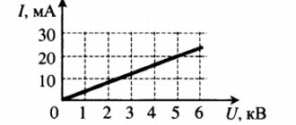
When the voltage of direct polarity is turned on, the direction of the external field is opposite to the direction of the contact field (Fig. 2.6). The width of the double layer will decrease, and a large forward current Ipr will arise in the circuit. Thus, the pn junction has pronounced one-way conductivity. This is expressed by its current-voltage characteristic (Fig. 2.7).
Rice. 2.7
When a forward voltage is applied to a pn junction, the current increases rapidly with increasing voltage. When a reverse voltage is applied to the pn junction, the current is very small, quickly reaches saturation and does not change up to a certain limit value of the reverse voltage Urev, after which it increases sharply. This is the so-called breakdown voltage, at which a breakdown of the pn junction occurs and it is destroyed. It should be noted that in Figure 2.7 the scale of the reverse current is a thousand times smaller than the scale of the forward current.
Brass Read more: Semiconductor diodes
Information about the work “Conductors, semiconductors and dielectrics”
Section: Physics Number of characters with spaces: 57947 Number of tables: 2 Number of images: 9
Similar works
Quantum yield of light-sensitive semiconductor-metal-dielectric structures
29489
0
6
..., no need to determine the thickness and resistivity of the metal layer, reducing the number of operations for processing the results. Claim of invention Method for determining efficiency photosensitive semiconductor-metal systems, including sequential deposition of a metal layer (in the form of a snake) 200 nm thick, a diiodide layer...
Crystals in nature
169673
2
43
... we must keep in mind the possibility of structural features of time for each of these types. II Interaction forces and the structure of crystals 2.1. The nature of binding forces in crystals. Different types of crystals and the possible location of nodes (the point around which an atom (molecule) vibrates) in a spatial lattice...
Electrical materials
26450
0
4
... types of processing in the manufacture of necessary products from them. Therefore, different materials have to be selected for different applications. Electrical insulating materials form the most numerous section of electrical materials in general; the number of individual types of specific electrical insulating materials used in the modern electrical industry amounts to many thousands...
Lectures on solid-state electronics
193480
0
0
... relevant computer programs. Similarly, for n of type n>>p For p, the following equations will correspondingly take place: (1.69)Voronkov E.N. Solid State Electronics. 2002 Contents Lecture 6 67 2. DIODES. 67 2.1. Semiconductor diodes with electron-hole junction (pn junction). 67 2.2. Electron-hole transition (pn – transition). The emergence...
Transistors.
pn
-Transitions are also used in transistors and more complex transistor structures - integrated circuits.
In a bipolar transistor, both electrons and holes serve as charge carriers. It contains two closely spaced transitions connected towards each other, which thereby form three separate pnp
- or
n-pn
structures.
In a pnp
transistor
the p
region serving as the input layer is called the emitter;
the central n
-region is the base;
The p
-region that serves as the output is called the collector.
In an n-pn
transistor,
the p-
and
n
-regions change places.
In a pnp
transistor, holes are injected through the forward biased emitter junction and collected at the reverse biased collector junction;
in an n-pn
device the same thing happens with electrons. The amount of charge carriers injected and collected can be varied by changing the small current supplied to the base region.
The field effect transistor is a unipolar device; this means that only the main type of charge carriers - either electrons in regions with conductivity n
-type, or holes in areas with
p
-type conductivity - pass through the conducting channel of the device. The current in the channel is changed by an electric field created by a voltage applied to the junction (reverse biased) or to the insulating layer on the surface of the device.
A bipolar transistor is essentially a current-controlled device, while a field-effect transistor is a voltage-controlled device. Both types of transistors are widely used in microelectronic circuits. see also
INTEGRATED CIRCUIT; TRANSISTOR.
Physical Basics
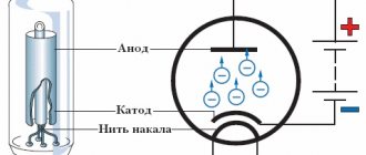
Development of P. e. made possible thanks to funds. achievements in the field of quantum theory of solids and PP physics. The operation of PP electronic devices and devices is based on the following most important properties of semiconductors and electronic processes in them: the simultaneous existence of two types of mobile charge carriers (negative - conduction electrons and positive - holes), which determine two types of electrical conductivity - electronic and hole; strong dependence of the magnitude and type of electrical conductivity on the concentration and type of impurity atoms; high sensitivity of PP properties to light, heat, electricity. and magnetic fields, mechanical. voltages (see, for example, Thermoelectric phenomena, Hall effect); occurrence at the border of areas of PP with decomposition. types of electrical conductivity or in a metal-semiconductor contact, respectively, an electron-hole junction (see p–n junction) or a Schottky barrier, which have almost one-sided conductivity; the ability of p–n junctions to inject charge carriers from the region where they are majority to the region in which they are minority, when the voltage is turned on in the direction of current flow through the junction; tunneling transition of carriers through a potential barrier, avalanche multiplication of charge carriers in strong electric. fields, the transition of carriers from one energy valley. zones to another with a change in their effective masses and mobility, which underlies the Gunn effect, etc.
Decisive for P. e. has a transistor effect (the effect of controlling the current of a gated junction using the current of an unlocked junction), as well as the effect of modulation by the conductivity field of a thin layer of semiconductor (channel). It is on the basis of these effects that bipolar and field-effect transistors operate, which determined fundamental changes in radio-electronic and other equipment and ensured the widespread use of automatic systems. management in technology.
pnpn-Devices.
In Fig. Figure 2 shows a four-layer structure called a triode thyristor (SCR). This is the most important type of device with pnpn
. Other devices with this structure are double-terminal and double-ended diodes.
The thyristor is an efficient switch that can handle significant power levels. With forward voltage on the thyristor, transition B
is biased in the opposite direction, so there is practically no current through it.
But when the forward bias voltage increases to a certain critical level,
an avalanche process develops
B. Charge carriers are then injected into the middle regions of N
and
P
, causing hole diffusion at the transition
A of the p-np
structure and electron diffusion at the transition of
the C n-pn
structure.
As a result, the current increases and the voltage drop across the device becomes small. This process can be initiated at a lower forward bias by injecting a small current into one of the p
of the control electrode. It follows that the SCR can serve as a nearly ideal switch, in which virtually no current flows in the off state, but a significant current flows in the open state at low voltage. SCR devices are widely used in motor and furnace control circuits, lighting controls and other applications.
Characteristics of the substance
Semiconductors can be divided into the following subgroups:
- Electronic (type n),
- Hole (type p).
Important! In substances of the n type, electrons can be considered as carriers, which, when a current occurs, move throughout the semiconductor in a chaotic manner.
What do semiconductor devices look like?
In the hole form p, so-called holes are considered as charge carriers (they mean free space between atoms, which can be replaced by another electron). Holes are considered to be equivalent to a positive charge. When a current occurs inside a conductor of type p, electrons perform only directed jumps between nearby atoms.
Important! When a charge jumps from one hole to another, the hole moves in the opposite direction, which entails the formation of a current.
You might be interested in: Features of megawatts and kilowatts
Ultrahigh frequency devices.
Transistors are widely used in microwave technology. In addition, ultrahigh frequencies can be generated using semiconductor components that have only two terminals, but have negative resistance, like tunnel diodes. The most common microwave devices of this type include avalanche diodes and Gunn diodes.
In an avalanche diode with avalanche breakdown in reverse biased pn
-transition, excess carriers appear in the drift region, i.e. in the region where charge carriers move under the influence of an applied voltage. If the size of the drift region is chosen correctly, then excess carriers pass through it during the negative half-cycle of the alternating current voltage. Further, the current increases as the voltage decreases. In this case, there is a kind of negative conductivity that can be used in a cavity resonator to generate microwave oscillations.
The operating principle of a Gunn diode is based on the property of semiconductors such as GaAs and InP to slow down electrons in the material at a certain critical electric field strength. In accordance with Ohm's law, the current in weak fields is proportional to the field strength. However, at very strong fields (with a strength of the order of several thousand volts per centimeter), the energies of the electrons in GaAs or InP increase to values at which the freedom of movement of electrons in the semiconductor crystal is limited. Due to their reduced mobility, when the electric field strength exceeds a certain critical level, the electrons slow down even more. As in an avalanche diode, there is some form of negative conductivity that can be used to generate microwave oscillations. see also
ULTRA-HIGH FREQUENCY RANGE.