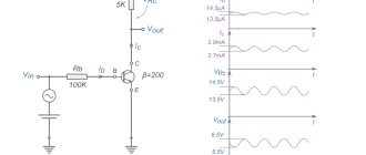
Semiconductor conduction mechanism
In a semiconductor crystal, each atom is bonded to four neighboring atoms by two-electron covalent bonds. As the temperature increases, according to the formulas of thermodynamics, some electrons in bonds receive such high energy that they can leave the bond and move into the space between other atoms, becoming free. This type of conductivity is called electronic conductivity.
In the bond that this electron left, there appears to be a “vacant” place. This connection is called a hole. Since when approaching an atom, an electron can continue to move along any of the four bonds - a hole can be occupied by another electron, while a hole is formed in another bond - will move in the opposite direction. It turns out that the hole can also move, transferring charge. This type of conductivity is called hole conductivity.
Rice. 1. Electronic and hole conductivity of a semiconductor.
Type n semiconductors
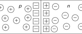
The introduction of impurities into a semiconductor significantly affects the behavior of electrons and the energy levels of the crystal spectrum. The valence electrons of impurity atoms create energy levels in the band gap of the spectrum. For example, if in the germanium lattice one atom is replaced by a pentavalent fluorine atom, then the energy of the additional electron will become less than the energy that corresponds to the lower boundary of the conduction band. The energy levels of such impurity electrons are below the bottom of the conduction band. These levels filled with electrons are called donor levels. To transfer electrons from donor levels to the conduction band, the energy required is less than that of a pure semiconductor. After electrons are transferred to the conduction band from donor levels, they say that n-type conductivity has appeared in the semiconductor. Semiconductors with a donor impurity are called electronic (donor) or n-type (negative) semiconductors. Electrons in n-type semiconductors serve as the majority charge carriers, while holes serve as minority charge carriers. The energy diagram of such a semiconductor is shown in Fig. 1.
Finished works on a similar topic
Course work Semiconductors of p and n type, pn junction 400 ₽ Abstract Semiconductors of p and n type, pn junction 220 ₽ Test work Semiconductors of p and n type, pn junction 250 ₽
Get completed work or advice from a specialist on your educational project Find out the cost
Impurity conductivity
The types of conductivity considered are the types of intrinsic conductivity of a semiconductor. This conductivity is low, since as the temperature increases, bond breakdowns occur in the crystal, which can irreversibly destroy the entire crystal. As a rule, this occurs at temperatures of the order of 370-400K.
To increase the conductivity of a semiconductor, you can do it differently - create a crystal lattice in which ready-made carriers will immediately be available.
To create a crystal lattice with a large number of carriers, when growing a semiconductor crystal, special impurity substances are added to it. Therefore, such conductivity is called impurity.
A crystal lattice with impurity conductivity can be created in two ways.
Donor conductivity
In tetravalent silicon, all electrons participate in creating covalent bonds in the crystal. If some atoms in the crystal are pentavalent, one electron of these atoms will not participate in bonds. As a result, it will be much weaker bound to its atom, its mobility will be higher even without an increase in temperature.
Impurity conductivity of a semiconductor, in which pentavalent atoms are a source of free electrons, is called donor conductivity.
Pentavalent arsenic or antimony are most often used as donor impurities.
Semiconductors having donor impurity conductivity are called n-type semiconductors.
Rice. 2. Semiconductor donor impurity.
Acceptor conductivity
Another option for impurity conductivity is the addition of trivalent atoms to the crystal. In this case, one of the bonds of the trivalent atom will be one-electron. A hole is formed that can be filled with electrons from neighboring atoms.
The impurity conductivity of a semiconductor, in which trivalent atoms form holes in the crystal, is called acceptor conductivity.
Trivalent indium or gallium are most often used as acceptor impurities.
Semiconductors having acceptor impurity conductivity are called p-type semiconductors.
Rice. 3. Acceptor impurity of a semiconductor.
It is not uncommon to add both types of impurities to a semiconductor. The general type of conductivity of such a crystal is determined by the impurity whose concentration is higher.
Impurity semiconductors
semiconductors
In the article conductivity of semiconductors, we found out that in a pure (intrinsic) semiconductor, the movement of charge carriers is carried out due to the processes of thermal generation and recombination.
In doped semiconductors, charge carriers are created due to an impurity introduced into the crystal. This is done in order to create a semiconductor with electron or hole conductivity. In a semiconductor of electronic conductivity (n-type), the main charge carriers are electrons, and in a semiconductor of hole conductivity (p-type), the main charge carriers are holes.
To create n -type semiconductor , a donor impurity . It is called a donor because it adds electrons to the crystal structure. For example, if you introduce an atom of an element from group 5 of the periodic table into silicon, you will get an excess electron. This will happen because silicon, which has 4 valence electrons, forms a covalent bond with only 4 electrons of phosphorus, which has 5 valence electrons. It turns out that one electron will be weakly connected to its atom, and even a small impact is enough for it to leave it and move into the conduction band. In this case, the impurity atom becomes a positive ion.
Excess electrons in the energy diagram are located in the so-called local valence levels . These levels are located in the band gap very close to the conduction band. In order to get into it, electrons at the local level need to receive about 0.1 eV. It turns out that the conduction band contains mainly electrons created by the impurity, since it is easier for them to move into it than for those electrons that are in the valence band and which need to cross the entire band gap. Therefore, there are many times more electrons than holes, and they are the majority carriers , and holes are minority carriers .
To create p semiconductor , an acceptor impurity is introduced into the crystal . For example, if you introduce an indium atom into a germanium crystal, the result will be a positive uncompensated charge. This will happen because germanium has 4 valence electrons, and indium 3. Indium forms a covalent bond with the three nearest germanium atoms, and one bond will be broken and a hole will remain in its place. With a slight increase in temperature, neighboring electrons will occupy this hole, but they themselves will leave it in another place. This will result in the movement of a positive charge. The figure shows where a hole can be located in an impurity atom and an electron, which will take its place with increasing temperature.
In the energy diagram, acceptor impurity holes create local valence levels in the band gap, near the valence band. The energy required for electrons to move to local levels is extremely small, therefore, when exposed to temperature, they all turn out to be filled with electrons transferred from the valence band. In this regard, the concentration of holes caused by the acceptor impurity increases in the valence band. Therefore, the majority charge carriers in a semiconductor are the holes formed by the impurity, and the electrons are the minority carriers.
The concentration of charge carriers depends on temperature. At the lowest temperatures, impurity electrons begin to pass into the conduction band. This continues up to a certain value until all the electrons have transferred. Then, with a further increase in temperature, the process of thermal generation begins to occur and new electrons and holes are formed. Ultimately, it may become so that the number of holes will approximately correspond to the number of electrons, in other words, degeneration of the semiconductor .
2.43 (15 Votes)
- Back
- Forward
- Views:
Intrinsic conductivity of semiconductors
In semiconductors, the main band is separated from the band of excited levels by a finite energy interval ($\triangle E$).
The main band of a semiconductor is called the valence band, and the band of excited states is called the conduction band. At T=0 K, the valence band is completely filled, while the conduction band is free. Therefore, near absolute zero, semiconductors do not conduct current. Generally speaking, dielectrics and semiconductors differ from the point of view of band theory only in the band gap ($\triangle E$). Conventionally, dielectrics include semiconductors with $\triangle E>2eV.$ Note 1
In semiconductors, as the temperature increases, electrons exchange energy with ions in the crystal lattice. Because of this, the electron can acquire additional kinetic energy of size $\approx kT.\ $This energy may be enough to transfer some of the electrons to the conduction band. These electrons in the conduction band conduct current.
Help with student work on the topic Intrinsic and impurity conductivity of semiconductors
Coursework 460 ₽ Essay 260 ₽ Test paper 210 ₽
Get completed work or consultation with a specialist on your educational project Find out the cost
In the valence band, quantum states that are not occupied by electrons are released. Such states are called holes. Holes are current carriers. Electrons can recombine with holes (make quantum transitions to unfilled states, that is, holes). In this case, the former filled states are released, that is, they become holes. The latter recombine with new electrons, and holes are formed again. As a result of these processes, an equilibrium concentration of holes is established; this concentration is the same throughout the entire volume of the conductor if there is no external field. The quantum transition of an electron is accompanied by its movement against the field. It reduces the potential energy of the system. A transition associated with movement in the direction of the field increases the potential energy of the system. Transitions against the field dominate over transitions along the field, which means that current will begin to flow through the semiconductor in the direction of the applied electric field. In an open semiconductor, current will flow until the electric field compensates for the external field. The final result of the phenomenon is the same as if the current carriers were not electrons, but positively charged holes. Consequently, a distinction is made between electron and hole conductivity of semiconductors.
Have questions about this topic? Ask a question to the teacher and get an answer in 15 minutes! Ask a Question
The true current carriers in metals and semiconductors are electrons; holes are introduced formally. Holes, like real positively charged particles, do not exist. However, it turned out that in an electric field, holes move in the same way as positively charged particles would move under classical consideration. Due to the small concentration of electrons in the conduction band and holes in the valence band, classical Boltzmann statistics can be used.
Note 2
The conductivity of semiconductors, both electronic and hole, is not related to the presence of impurities. It is called the intrinsic electrical conductivity of semiconductors.
In an ideally pure semiconductor without any impurities, each electron released by thermal movement or light would correspond to the formation of one hole, that is, the number of electrons and holes that participate in the creation of current would be the same.
Ideally pure semiconductors do not exist in nature; making them artificially is extremely difficult. Small traces of impurities qualitatively change the properties of semiconductors.
Impurity conductivity of semiconductors
The conductivity of semiconductors caused by impurities is called impurity conductivity , and the semiconductors themselves are called impurity semiconductors . Impurity conductivity is caused by impurities (atoms of foreign elements), as well as defects such as excess atoms (compared to the stoichiometric composition), thermal (empty sites or atoms in interstices) and mechanical (cracks, dislocations, etc.) defects. The presence of an impurity in a semiconductor significantly changes its conductivity. For example, when approximately 0.001 at.% boron is introduced into silicon, its conductivity increases by approximately 106 times.
In semiconductors with an impurity whose valency is one unit greater than the valence of the main atoms, the current carriers are electrons; electronic impurity conductivity (n-type conductivity) occurs . Semiconductors with such conductivity are called electronic (or n-type semiconductors ). Impurities that are a source of electrons are called donors , and the energy levels of the remaining impurities are called donor levels .
For example, when a germanium atom is replaced by a pentavalent arsenic atom (Fig. 22, a), one electron cannot form a covalent bond; it turns out to be redundant and can easily be split off from the atom during thermal vibrations of the lattice, i.e., become free. The formation of a free electron is not accompanied by a violation of the covalent bond; therefore, unlike the case considered earlier, a hole does not appear. The excess positive charge that appears near the impurity atom is bound to the impurity atom and therefore cannot move along the lattice.
Rice. 22
From the point of view of band theory, the considered process can be represented as follows (Fig. 22, b). The introduction of an impurity distorts the lattice field, which leads to the appearance of arsenic valence electrons in the band gap energy level D of arsenic valence electrons, called an impurity level. In the case of germanium with an admixture of arsenic, this level is located from the bottom of the conduction band at a distance of ΔЕD = 0.013 eV. Since ΔЕD< kT, then even at ordinary temperatures the energy of thermal motion is sufficient to transfer electrons of the impurity level to the conduction band; the positive charges formed in this case are localized on the stationary arsenic atoms and do not participate in conductivity.
In semiconductors with an impurity whose valence is one less than the valence of the main atom, the current carriers are holes; hole conductivity (p-type conductivity) occurs Semiconductors with such conductivity are called hole (or p-type semiconductors). Impurities that capture electrons from the valence band of a semiconductor are called acceptors, and the energy levels of these impurities are called acceptor levels.
Let us assume that an impurity atom with three valence electrons, for example boron, is introduced into the silicon lattice (Fig. 23, a). To form bonds with four nearest neighbors, the boron atom lacks one electron; one of the bonds remains incomplete and the fourth electron can be captured from a neighboring atom of the main substance, where a hole is accordingly formed. The sequential filling of the resulting holes with electrons is equivalent to the movement of holes in the semiconductor, i.e. the holes do not remain localized, but move in the silicon lattice as free positive charges. The excess negative charge that arises near the impurity atom is associated with the impurity atom and cannot move along the lattice.
a) b)
Rice. 23
According to the band theory, the introduction of a trivalent impurity into the silicon lattice leads to the appearance of an impurity energy level A in the band gap, which is not occupied by electrons. In the case of silicon with boron impurity, this level is located above the upper edge of the valence band at a distance of ΔEA = 0.08 eV (Fig. 23, 6). The proximity of these levels to the valence band leads to the fact that even at relatively low temperatures, electrons from the valence band move to impurity levels and, binding to boron atoms, lose the ability to move along the silicon lattice, i.e., they do not participate in conductivity. Current carriers are only holes that appear in the valence band.
In contrast to intrinsic conductivity, which is carried out simultaneously by electrons and holes, impurity conductivity of semiconductors is mainly due to carriers of the same sign: electrons in the case of a donor impurity, holes in the case of an acceptor impurity. These current carriers are called main carriers. In addition to the majority carriers, a semiconductor also contains minority carriers: in n-type semiconductors there are holes, in p-type semiconductors there are electrons.
The presence of impurity levels in semiconductors significantly changes the position of the Fermi level EF. Calculations show that in the case of n-type semiconductors, the Fermi level EF at 0 K is located in the middle between the bottom of the conduction band and the donor level (Fig. 24a). With increasing temperature, an increasing number of electrons move from donor states to the conduction band, but, in addition, the number of thermal fluctuations that can excite electrons from the valence band and transfer them across the energy gap also increases. Therefore, at high temperatures, the Fermi level tends to shift downward (solid curve) to its limiting position at the center of the band gap, characteristic of the intrinsic semiconductor.
Rice. 24
The Fermi level in p-type semiconductors at 0 K is located in the middle between the top of the valence band and the acceptor level (Fig. 24, b). The solid curve again shows its displacement with temperature. At temperatures at which impurity atoms are completely depleted and the carrier concentration increases due to the excitation of intrinsic carriers, the Fermi level is located in the middle of the band gap, as in an intrinsic semiconductor.
The conductivity of an impurity semiconductor, like the conductivity of any conductor, is determined by the concentration of carriers and their mobility. With a change in temperature, the mobility of carriers changes according to a relatively weak power law, and the concentration of carriers - according to a very strong exponential law, therefore, the temperature dependence of the conductivity of impurity semiconductors is determined mainly by the temperature dependence of the concentration of current carriers in it. In Fig. Figure 25 shows an approximate graph of the dependence of lnγ on 1/T for impurity semiconductors. Section AB describes the impurity conductivity of the semiconductor.
The increase in impurity conductivity of a semiconductor with increasing temperature is mainly due to an increase in the concentration of impurity carriers. Section BC corresponds to the region of impurity depletion (this is also confirmed by experiments), section CD describes the intrinsic conductivity of the semiconductor.
Rice. 25