Main characteristics and parameters of transistors
Classification of transistors. Conductivity, gain, parameters that determine power, permissible voltage, frequency and noise properties of the transistor.Transistor , in the general sense of the word, is a semiconductor device, usually with three terminals, capable of amplifying the signal supplied to it. Performing the functions of amplification, conversion, generation, and switching of signals in electrical circuits, the transistor is currently the basis of the vast majority of electronic devices and integrated circuits.
On circuit diagrams, the transistor is usually designated by the Latin letters “VT” or “Q” with the addition of a position number (for example, VT12 or Q12).
In domestic documentation of the last century, the designations “T”, “PP” or “PT” were used.
Two types of transistors are predominantly used in industrial and amateur radio designs - bipolar and field-effect. What are they?
BASIC CLASSIFICATION, PARAMETERS AND CHARACTERISTICS OF TRANSISTORS.
The main classification that determines the scope of application of transistors is based on: the source material on which they are made, the conductivity structure, the maximum permissible voltage, the maximum power dissipated at the collector, frequency properties, noise characteristics, the slope of the transfer characteristic (for field) or static coefficient current transmission (for bipolar transistors). Let us consider the listed classification points in more detail.
Based on the source semiconductor material, transistors are classified into: - germanium (not currently produced); — silicon (the most widely represented class); — from gallium arsenide (mainly microwave transistors), etc.
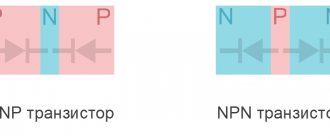
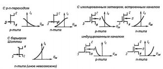
According to their structure, transistors are classified into: - pnp structures - bipolar transistors of “direct conduction”; — npn structures – bipolar transistors of “reverse conduction”; — p-type – field-effect transistors with “p-type conductivity”; - n-type – field-effect transistors with “n-type conductivity”. In turn, field-effect transistors are divided into devices with a control pn junction (JFET transistors) and insulated gate transistors (MIS or MOS transistors).
According to the power parameter, transistors are divided into: - low power transistors (conventionally Pmax - medium power transistors (0.3) - high power transistors (Pmax > 1.5 W). Also an indirect indicator of transistor power is the parameter of the maximum permissible collector current (Ik_max).
According to the parameter of the maximum permissible voltage Uke or Usi, transistors are divided into: - transistors for general use (conventionally Uke_max) - high-voltage transistors (Uke_max > 100 V). For modern bipolar and field-effect transistors, the parameter Uke_max (Usi_max) can reach several thousand volts!
According to frequency characteristics, transistors are divided into: - low-frequency transistors (conventionally Fgr - medium-frequency transistors (3 - high-frequency transistors (30 - ultra-high-frequency transistors (Fgr > 300 MHz); The main parameter characterizing the speed of the transistor is the cutoff frequency of the current transfer coefficient (Fgr). Indirect - input and output capacitances.For transistors designed for use in switching circuits, the switching delay parameter (tr and ts) can also be specified.
According to noise characteristics, transistors are divided into: - transistors with non-standardized noise figure; — transistors with normalized noise figure (Ksh).
The current transfer coefficient (h21 - for a bipolar transistor) and the slope of the transfer characteristic (S - for a field transistor) are one of the main parameters of a semiconductor. Both the quality indicators of the transistor amplifier stage and the requirements for the previous and subsequent stages depend on it.
However, let's consider this article introductory, and we will go deeper and discuss in detail the influence of certain parameters on the operation and behavior of a bipolar or field-effect transistor on the following pages. A complete list of articles devoted to the description of the operation of the transistor, as well as calculations of cascades on field-effect and bipolar semiconductors, is given in the section “This may also be interesting.”
Analysis of results
As can be seen from the results, VCmax turned out to be less than VCmin. This is because the voltage across resistor VRc is subtracted from the supply voltage VCC. However, in most cases this does not matter, since we are interested in the variable component of the signal - the amplitude, which has increased from 0.1V to 1V. The frequency and sinusoidal shape of the signal have not changed. Of course, a Vout/Vin ratio of ten times is far from the best indicator for an amplifier, but it is quite suitable for illustrating the amplification process.
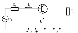
So, let's summarize the principle of operation of an amplifier based on a bipolar transistor. A current Ib flows through the base, carrying DC and AC components. A constant component is needed so that the PN junction between the base and emitter begins to conduct - “opens”. The variable component is, in fact, the signal itself (useful information). The collector-emitter current inside the transistor is the result of the base current multiplied by the gain β. In turn, the voltage across the resistor Rc above the collector is the result of multiplying the amplified collector current by the resistor value.
Thus, the Vout pin receives a signal with an increased oscillation amplitude, but with the same shape and frequency. It is important to emphasize that the transistor takes energy for amplification from the VCC power source. If the supply voltage is insufficient, the transistor will not be able to operate fully, and the output signal may be distorted.
Operating modes of a bipolar transistor
In accordance with the voltage levels on the electrodes of the transistor, there are four modes of its operation:
Cut off mode.
Active mode.
Saturation mode.
Inverse mode (reverse mode).
When the base-emitter voltage is lower than 0.6V - 0.7V, the PN junction between the base and emitter is closed. In this state, the transistor has no base current. As a result, there will be no collector current either, since there are no free electrons in the base ready to move towards the collector voltage. It turns out that the transistor is, as it were, locked, and they say that it is in cutoff mode
.
In active mode
The voltage at the base is sufficient for the PN junction between the base and emitter to open. In this state, the transistor has base and collector currents. The collector current equals the base current multiplied by the gain. That is, the active mode is the normal operating mode of the transistor, which is used for amplification.
Sometimes the base current may be too high. As a result, the supply power is simply not enough to provide such a magnitude of collector current that would correspond to the gain of the transistor. In saturation mode, the collector current will be the maximum that the power supply can provide and will not depend on the base current. In this state, the transistor is not able to amplify the signal, since the collector current does not respond to changes in the base current.
In saturation mode, the conductivity of the transistor is maximum, and it is more suitable for the function of a switch (switch) in the “on” state. Similarly, in the cut-off mode, the conductivity of the transistor is minimal, and this corresponds to the switch in the off state.
In this mode, the collector and emitter change roles: the collector PN junction is biased in the forward direction, and the emitter junction is biased in the opposite direction. As a result, current flows from the base to the collector. The collector semiconductor region is asymmetrical to the emitter, and the gain in inverse mode is lower than in normal active mode. The transistor is designed in such a way that it operates as efficiently as possible in active mode. Therefore, the transistor is practically not used in inverse mode.
Basic parameters of a bipolar transistor.
Current gain
– ratio of collector current IC to base current IB.
Denoted β
,
hfe
or
h21e
, depending on the specifics of the calculations carried out with transistors.
β is a constant value for one transistor, and depends on the physical structure of the device. A high gain is calculated in hundreds of units, a low gain - in tens. For two separate transistors of the same type, even if they were “pipeline neighbors” during production, β may be slightly different. This characteristic of a bipolar transistor is perhaps the most important. If other parameters of the device can often be neglected in calculations, then the current gain is almost impossible.
Input impedance
– resistance in the transistor that “meets” the base current.
Denoted by R in
(
R in
). The larger it is, the better for the amplification characteristics of the device, since on the base side there is usually a source of a weak signal, which needs to consume as little current as possible. The ideal option is when the input impedance is infinity.
Rin for an average bipolar transistor is several hundred KΩ (kilo-ohms). Here the bipolar transistor loses very much to the field-effect transistor, where the input resistance reaches hundreds of GΩ (gigaohms).
Output conductivity
– conductivity of the transistor between collector and emitter. The greater the output conductance, the more collector-emitter current will be able to pass through the transistor at less power.
Also, with an increase in output conductivity (or a decrease in output resistance), the maximum load that the amplifier can withstand with insignificant losses in overall gain increases. For example, if a transistor with low output conductivity amplifies the signal 100 times without a load, then when a 1 KΩ load is connected, it will already amplify only 50 times. A transistor with the same gain but higher output conductance will have a smaller gain drop. The ideal option is when the output conductivity is infinity (or output resistance Rout = 0 (Rout = 0)).
Frequency response
– dependence of the transistor gain on the frequency of the incoming signal. As the frequency increases, the transistor's ability to amplify the signal gradually decreases. The reason for this is the parasitic capacitances formed in the PN junctions. The transistor does not react instantly to changes in the input signal in the base, but with a certain slowdown due to the time spent filling these containers with charge. Therefore, at very high frequencies, the transistor simply does not have time to react and fully amplify the signal.
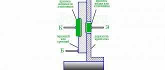
Bipolar transistor
- a three-electrode semiconductor device, one of the types of transistors. In the semiconductor structure, two pn junctions are formed, charge transfer through which is carried out by carriers of two polarities - electrons and holes. That is why the device was called “bipolar” (from the English bipolar), in contrast to a field-effect (unipolar) transistor.
It is used in electronic devices to amplify or generate electrical oscillations, and also as a switching element (for example, in TTL circuits).
Read also: How to install a digital receiver on your TV
Operating modes [edit | edit code]
| Voltages at emitter, base, collector (UE, UB, UC,U_ ,U_>) | Base-emitter junction bias for npn type | Base-collector junction offset for npn type | Mode for npn type |
| UEUBUC | direct | the opposite | normal active mode |
| U_>»> UEUB > UC U_> U_>»/> | direct | direct | saturation mode |
| U_UE > UBUC >U_ U_ | the opposite | the opposite | cut-off mode |
| U_ >U_>»> UE > UB > UC >U_ >U_> U_ >U_>»/> | the opposite | direct | inverse active mode |
| Voltages at emitter, base, collector (UE, UB, UC,U_ ,U_>) | Base-emitter junction bias for pnp type | Base-collector junction offset for pnp type | Mode for pnp type |
| UEUBUC | the opposite | direct | inverse active mode |
| U_>»> UEUB > UC U_> U_>»/> | the opposite | the opposite | cut-off mode |
| U_UE > UBUC >U_ U_ | direct | direct | saturation mode |
| U_ >U_>»> UE > UB > UC >U_ >U_> U_ >U_>»/> | direct | the opposite | normal active mode |
Normal active mode [edit | edit code]
The emitter-base junction is switched on in the forward direction [2] (open), and the collector-base junction is switched on in the reverse direction (closed):
Inverse active mode [edit | edit code]
The emitter junction is reverse biased, and the collector junction is forward biased: UKB>
0;
UEB Saturation mode [edit |
edit code ] Both pn
transitions are shifted in the forward direction (both are open).
If the emitter and collector p-n
junctions are connected to external sources in the forward direction, the transistor will be in saturation mode.
The diffusion electric field of the emitter and collector junctions will be partially weakened by the electric field created by external sources Ueb
and
Ukb
.
As a result, the potential barrier that limited the diffusion of the main charge carriers will decrease, and the penetration (injection) of holes from the emitter and collector into the base will begin, that is, currents called saturation currents of the emitter ( I E.
us) and collector (
I
K. us).
Collector-emitter saturation voltage
(UKE. us) is the voltage drop across an open transistor (semantic analogue
of RSI. open
for field-effect transistors).
Similarly, the base-emitter saturation voltage
(UBE.us) is the voltage drop between the base and emitter across an open transistor.
Cutoff mode [edit | edit code]
In this mode, the collector pn
the junction is reverse biased, and both reverse and forward bias can be applied to the emitter junction, not exceeding the threshold value at which the emission of minority charge carriers into the base region from the emitter begins (for silicon transistors approximately 0.6-0.7 IN).
The cutoff mode corresponds to the condition U
EB [5] [6] .
Barrier mode [edit | edit code]
In this mode the base
The direct current transistor is connected short-circuited or through a small resistor to its
collector
, and
a resistor is connected the collector
or
emitter In this connection, the transistor is a kind of diode connected in series with a current-setting resistor. Such cascade circuits are distinguished by a small number of components, good high-frequency isolation, a large operating temperature range, and insensitivity to transistor parameters.
Read also: How to sharpen hairdressing scissors at home