Field effect transistors
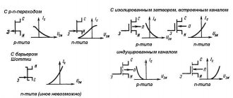
Field effect transistors (FET, Field Effect Transistor) have the same purpose, but differ in internal structure. A particular type of these components are MOSFET (Metal-Oxide-Semiconductor Field Effect Transistor) transistors. They allow you to operate with much greater power with the same dimensions. And the control of the “damper” itself is carried out exclusively using voltage: no current flows through the gate, unlike bipolar transistors.
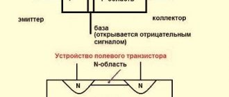
Field effect transistors have three contacts:
N-Channel and P-Channel
By analogy with bipolar transistors, field transistors differ in polarity. The N-Channel transistor was described above. They are the most common.
P-Channel when designated differs in the direction of the arrow and, again, has an “inverted” behavior.
How to distinguish a bipolar transistor from a field effect transistor
- Active mode of operation of a bipolar transistor
- Bipolar transistors. Operating principle, static and dynamic parameters of transistors.
- Dynamic parameters of a field-effect transistor
- Differential parameters of field-effect transistors with a control pn junction. Temperature dependence of field-effect transistor parameters.
- E. Kovalenko: They receive the same policy as everyone else, it is no different from the policy of any household person.
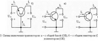
- STUDY OF TYPICAL TRANSISTOR CONNECTION CIRCUITS
- CASCADE ON BIPOLAR TRANSISTORS
- Small-signal models and parameters of MIS transistors. Frequency characteristics. Circuits for connecting an MIS transistor with an induced channel.
- Mineral composition: feldspar and augite
- Organization of field practice
- Basic parameters of the field-effect transistor amplifier stage
- Field Practice Report
What parameters determine the properties of a transistor in its performance?
The transistors operate between the active mode and the cutoff mode, as a result of which the circuit does not enter saturation mode, which increases its performance.
The performance of the transistor depends only on the rate of recharging of the barrier capacitance. The reason for the inertia of a bipolar transistor is the finite time of charge transfer from the emitter junction to the collector and the parasitic capacitances of these junctions. And the performance, in turn, depends on how strong the inertial properties are.
The speed of the transistor is determined by the switching time of the transistor switches, and the specific conductivity (and speed) depends on the concentration of charge carriers and their mobility.
The speed of the transistor is determined by the switching time of the transistor switches, or valves, which is inversely proportional to the power consumption P: = A/P. Here A is the key operation for one switching. Increasing power in order to speed up switching, as a rule, requires increasing the distance between individual circuit elements to maintain the required thermal conditions, which leads to a decrease in the density of the elements and an increase in the delay in signal propagation along the lines.
The power dissipated in the crystal as heat must be less than the thermal power that can be removed.
A field-effect transistor differs from a bipolar transistor, firstly, in its operating principle: in a bipolar transistor, the output signal is controlled by the input current, and in a field-effect transistor, by the input voltage or electric field. Secondly, field-effect transistors have significantly higher input resistances, which is associated with the reverse bias of the gate pn junction in the type of field-effect transistors under consideration. Thirdly, field-effect transistors can have a low noise level (especially at low frequencies), since field-effect transistors do not use the phenomenon of injection of minority charge carriers and the field-effect transistor channel can be separated from the surface of the semiconductor crystal. The processes of carrier recombination in the pn junction and in the base of the bipolar transistor, as well as generation-recombination processes on the surface of the semiconductor crystal, are accompanied by the appearance of low-frequency noise.
| Rice. 4.4. Active mode of bipolar transistor |
Date added: 2015-04-24 ; ; Copyright infringement? ;
Your opinion is important to us! Was the published material useful? Yes | No
The transistor is a ubiquitous and important component in modern microelectronics. Its purpose is simple: it allows you to control a much stronger one using a weak signal.
In particular, it can be used as a controlled “damper”: by the absence of a signal at the “gate”, block the flow of current, and by supplying it, allow it. In other words: this is a button that is pressed not by a finger, but by applying voltage. This is the most common application in digital electronics.
Transistors are available in different packages: the same transistor can look completely different in appearance. In prototyping, the most common cases are:
The designation on the diagrams also varies depending on the type of transistor and the designation standard used in the compilation. But regardless of the variation, its symbol remains recognizable.
Differences between field-effect transistors and bipolar ones. Areas of use
As mentioned above, the first and main difference between these two types of transistors is that the latter are controlled by changing the current, and the former by voltage. And from this follow other advantages of field-effect transistors compared to bipolar ones:
· high input impedance for direct current and at high frequency, hence low control losses;
· high performance (due to the absence of accumulation and resorption of minor carriers);
· since the amplifying properties of field-effect transistors are determined by the transfer of majority charge carriers, their upper limit of effective gain is higher than that of bipolar ones;
· high temperature stability;
· low noise level, since field-effect transistors do not use the phenomenon of injection of minority charge carriers, which makes bipolar transistors “noisy”;
· low power consumption.
However, with all this, field-effect transistors also have a drawback - they are “afraid” of static electricity, therefore, when working with them, they have particularly stringent requirements for protection from this scourge.
Where are field-effect transistors used? Yes, almost everywhere. Digital and analog integrated circuits, tracking and logical devices, energy-saving circuits, flash memory... Why, even quartz clocks and TV remote control work on field-effect transistors.
Fully controllable high power transistor switches
A key assembled on a transistor is called a transistor switch . The transistor switch performs only two operations: ON and OFF ; we will consider the intermediate mode between “on” and “off” in the following chapters. An electromagnetic relay performs the same function, but its switching speed is very slow from the point of view of modern electronics, and the switching contacts wear out quickly.
What is a transistor switch? Let's take a closer look:
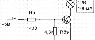
This is a familiar pattern, isn't it? Everything here is elementary and simple: we apply a voltage of the required nominal value to the base and current begins to flow through the circuit from the positive terminal +Bat2—>light bulb—>collector—>emitter—>to the negative terminal Bat2. The voltage on Bat2 must be equal to the operating voltage of the light bulb. If everything is so, then the light bulb emits light. Instead of a light bulb there may be some other load. Resistor "R" is required here in order to limit the value of the control current at the base of the transistor.
But is everything as simple as it seems at first glance?
So, let's remember what requirements must be in order to completely “open” the transistor? We read the article on the principle of amplification of a bipolar transistor and remember:
1) In order to fully open the transistor, the base-emitter voltage must be greater than 0.6-0.7 Volts.
2) The current flowing through the base must be such that the electric current can flow through the collector-emitter absolutely unimpeded.
Ideally, the resistance through the collector-emitter should be zero, but in reality it will be fractions of an Ohm.
This mode is called “ saturation mode ”.
This drawing is the imagination of my mind. Here I drew the same saturation mode.
As we can see, the collector and emitter are short-circuited in saturation mode, so the light bulb burns at full power.
Now what needs to be done to prevent the light from burning at all? Can I turn it off manually? For what? After all, we have a controllable resistor: a collector-emitter, the resistance of which we can change by passing a certain current through the base. So, what is needed for the light bulb to stop burning altogether? There are two possible ways:
First way . Completely disconnect power from the base resistor, as in the figure below.
In reality, the base output is a kind of small antenna that can receive various interference and interference from the surrounding space. From these interferences, a small current may begin to flow in the base. And as you remember, in order to open a transistor you don’t need much. And it may even happen that the light bulb glows very quietly! How to get out of this situation? Yes, very easy! It is enough to place a resistor between the base and the emitter, that is, to make sure that when the voltage is turned off, the voltage at the base is zero. And which terminal of the transistor is below zero? Emitter! That is, in scientific language, we must make sure that the potential at the base is equal to the potential at the emitter.
So, should I now ground the base every time I turn it off? Ideally, yes. But there is a more cunning solution. It is enough to place a resistor between the base and emitter. Its value is generally taken to be approximately 10 times higher than the value of the base resistor.
Since there is one more resistor in the circuit, we will call the base resistor RB, and we will not invent a resistor between the base and emitter and will call it RBE. The diagram will look like this:
How does the resistor RBE behave in a circuit? If switch S is closed, then this resistor does not have any effect on the operation of the circuit, since an already small current flows through it, which controls the base. Well, if switch S is open, then, as I already said, the potential at the base will be equal to the potential of the emitter, that is, zero.
Second way. Achieve that UBE <0.6 Volts or that the base current IB = 0. This method is most often used in MK and other logic circuits.
In both the first and second cases, our transistor does not pass current through the collector-emitter. In this case, the transistor is said to be in cutoff .
Thyristors
Thyristor structure
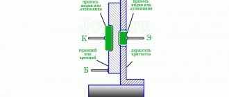
A thyristor is a four-layer semiconductor device, the layers are arranged in series, their conductivity types alternate: p‑n‑p‑n. p‑n‑junctions between layers in the figure are designated as “P1”, “P2” and “P3”. The contact connected to the outer p‑layer is called the anode, and to the outer n‑layer is called the cathode. In principle, a thyristor can have up to two control electrodes connected to the inner layers. But thyristors are usually manufactured with one control electrode, or without control electrodes at all (such a device is called a dinistor).
To turn on the thyristor, it is enough to briefly apply a signal to the control electrode - the thyristor will open and will remain in this state until the current through the thyristor becomes less than the holding current.
So, the main principle of operation of a thyristor and circuits based on it is that we open the thyristor by applying a signal to the control electrode, and close it by reducing the anode-cathode current.
As in a bipolar transistor, the main role in the principle of operation is played by minority charge carriers (MCC) and the reverse-biased pn junction. While there are few minor carriers, the transition is closed, but if you throw an NNZ to the transition, it will open. There are two main ways to add an NC in a thyristor: 1) pump current into the control electrode; 2) increase the voltage so much that an avalanche breakdown occurs.
10.5. Comparison of field-effect and bipolar transistors
Field-effect and bipolar transistors perform the same functions: they work in a circuit either as a linear amplifier or as a switch. Below (Table 10.4) is a brief general comparison of these two types of transistors.
Controlled physical process - injection of minority charge carriers: the control current changes - the flow of injected charge carriers changes, which leads to a change in the output current
A controlled physical process is a field effect that causes a change in the concentration of charge carriers in the channel: the control voltage changes - the conductivity of the channel changes, which leads to a change in the output current
The output current is provided by carriers of both signs (holes and electrons)
The output current is provided by the majority carriers of the same sign (either holes or electrons)
The device is controlled by current, since there is a forward biased pn
— transition and input resistance are low
The device is voltage controlled; the input resistance is very large, since the input circuit is isolated from the output circuit by reverse bias pn
- transition or dielectric layer
When controlled by integrated circuits, additional current amplification is required
Direct control from integrated circuits possible
Relatively low current gain
Very high current gain
The need for special measures to improve noise immunity
Low heat resistance: with increasing current, the temperature of the structure increases, which leads to a greater increase in current
High heat resistance: an increase in the temperature of the structure leads to an increase in channel resistance and the current decreases
High probability of self-heating and secondary breakdown
Low probability of self-heating and secondary breakdown
High sensitivity to current overloads
Low sensitivity to current overloads
The need to equalize currents in parallel connection of devices
Uniform current distribution in parallel connection of devices
The comparison shows that in discrete electronic devices, field-effect transistors are preferable to bipolar transistors in a number of applications. Firstly, the control circuit of field-effect transistors consumes negligible energy, since the input resistance of these devices is very high. As a rule, the power and current amplification in field-effect transistors is much greater than in bipolar ones. Secondly, due to the fact that the control circuit is isolated from the output circuit, the reliability of operation and noise immunity of field-effect transistor circuits are significantly increased. Thirdly, field-effect transistors have a low level of intrinsic noise, which is associated with the absence of injection and its inherent fluctuations. Finally, fourthly, field-effect transistors, generally speaking, have a higher operating speed, since they do not have inertial processes of accumulation and resorption of charge carriers.
However, field-effect transistors also have disadvantages. Due to the relatively high channel resistance in the on-state, the voltage drop across the on-field field effect transistor is noticeably greater than the voltage drop across the saturated bipolar transistor. This disadvantage is further aggravated by the fact that the temperature dependence of the channel resistance is stronger than the temperature dependence of the saturation voltage of the bipolar transistor.
Source