Features of the bipolar transistor device
A bipolar transistor includes three regions:
- emitter;
- the base is very thin, which is made of a lightly doped semiconductor, the resistance of this area is high;
- collector - its area is larger in size than the emitter area.
Metal contacts are soldered to each area, which serve to connect the device to the electrical circuit.
The collector and emitter conductivities are the same and opposite to the base conductivities. In accordance with the type of conductivity of the areas, pnp or npn devices are distinguished. The devices are asymmetrical due to the difference in contact area - between the emitter and base it is much lower than between the base and collector. Therefore, it is impossible to swap K and E by changing polarity.
The principle of operation of a bipolar transistor
This type of transistor has two junctions:
- electron-hole between the emitter and the base - emitter;
- between the collector and the base - collector.
The distance between transitions is small. For high-frequency parts it is less than 10 microns, for low-frequency parts – up to 50 microns. To activate the device, voltage is supplied to it from a third-party power supply. The operating principle of bipolar transistors with pnp and npn junctions is the same. Transitions can operate in forward and reverse directions, which is determined by the polarity of the applied voltage.
Design feature of a bipolar transistor
To produce a bipolar transistor, you need a semiconductor of hole or electronic conductivity type, which is obtained by diffusion or alloying with acceptor impurities. As a result, regions with polar conductivities are formed on both sides of the base.
Bipolar transistors are of two types based on conductivity: npn and pnp. The operating rules that govern a bipolar transistor with npn conductivity (for pnp it is necessary to change the polarity of the applied voltage):
- The positive potential at the collector is more important compared to the emitter.
- Any transistor has its own maximum permissible parameters Ib, Ik and Uke, exceeding which is in principle unacceptable, since this can lead to destruction of the semiconductor.
- The base-emitter and base-collector terminals function like diodes. As a rule, the diode in the base-emitter direction is open, and in the base-collector direction it is biased in the opposite direction, that is, the incoming voltage interferes with the flow of electric current through it.
- If steps 1 to 3 are completed, then the current Ik is directly proportional to the current Ib and has the form: Ik = he21*Ib, where he21 is the current gain. This rule characterizes the main quality of the transistor, namely that the low base current controls the powerful collector current.
For different bipolar transistors of the same series, the he21 indicator can fundamentally vary from 50 to 250. Its value also depends on the flowing collector current, the voltage between the emitter and the collector, and on the ambient temperature.
Let's study rule No. 3. It follows from this that the voltage applied between the emitter and the base should not be significantly increased, since if the base voltage is 0.6...0.8 V greater than the emitter (forward voltage of the diode), then an extremely large current will appear. Thus, in a working transistor, the voltages at the emitter and base are interconnected according to the formula: Ub = Ue + 0.6V (Ub = Ue + Ube)
Let us remind you once again that all these points apply to transistors with npn conductivity. For the pnp type everything should be reversed.
You should also pay attention to the fact that the collector current has no connection with the conductivity of the diode, since, as a rule, reverse voltage is supplied to the collector-base diode. In addition, the current flowing through the collector depends very little on the potential on the collector (this diode is similar to a small current source)
Transistor tester / ESR meter / generator
Multifunctional device for testing transistors, diodes, thyristors...
More details
Operating modes of bipolar transistors
Cut-off mode
The passages are closed, the device does not work. This mode is obtained when connecting back to external sources. Reverse small collector and emitter currents flow through both junctions. It is often believed that the device in this mode breaks the circuit.
Active inverse mode
Is intermediate. The B-K junction is open, and the emitter-base is closed. The base current in this case is significantly less than the E and K currents. The amplifying characteristics of the bipolar transistor in this case are absent. This mode is in little demand.
Saturation mode
The device is completely open. Both junctions are connected to current sources in the forward direction. This reduces the potential barrier limiting the penetration of charge carriers. Currents begin to flow through the emitter and collector, which are called “saturation currents”.
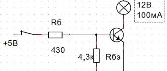
Switching circuits for bipolar transistors
Depending on the contact to which the power source is supplied, there are 3 schemes for switching on devices.
Common emitter
This circuit for connecting bipolar transistors provides the greatest increase in current-voltage characteristics (CV characteristics), therefore it is the most popular. The disadvantage of this option is the deterioration of the amplification properties of the device with increasing frequency and temperature. This means that for high-frequency transistors it is recommended to choose a different circuit.
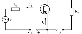
With a common base
Used for operation at high frequencies. The noise level is reduced, the gain is not very high. Cascades of devices assembled according to this scheme are in demand in antenna amplifiers. The disadvantage of this option is the need for two power sources.
With common collector
This option is characterized by the transmission of the input signal back to the input, which significantly reduces its level. The current gain is high and the voltage gain is low, which is a disadvantage of this method. The circuit is suitable for cascades of devices in cases where the input signal source has a high input impedance.
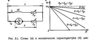
Basic circuits for connecting transistors
A transistor, as a semiconductor device with three electrodes (emitter, base, collector), can be turned on in three main ways (Fig. 3.1 - 3.6). As you know, the input signal enters the amplifier via two wires; The output signal is also routed through two wires. Consequently, for a three-electrode amplifying device, when an input signal is supplied and an output signal is received via two wires, one of the electrodes will certainly be common. According to which of the electrodes in the transistor switching circuit will be common, three main switching circuits are distinguished: with a common emitter (CE), a common collector (CC) and a common base (CB).
Rice. 3.1. Common emitter (CE) circuit
Rice. 3.2. Circuit with a common collector (OK)
Practical variants of switching circuits for transistors of the p-p-p and p-p-p structures are shown in Fig. 3.1 - 3.6. As follows from a comparison of the figures, these circuits are identical and differ only in the polarity of the supplied voltage.
To determine the input (RBX.) and output (RBbix.) resistance of each of the switching circuits, as well as the amplification factors for current (K,), voltage (Ki) and power (KR = K|ХKi), calculated and experimental values and formulas are given in tables 3.1 and 3.2.
The table with formulas is given for approximate calculations, and for the initial, primary assessment and comparison of the properties of the main circuits for connecting transistors, a second table with numerical estimates is intended.
Rice. 3.3. Common base (CB) scheme
The designations in the table are as follows: RH - load resistance; R3 is the emitter resistance or the ratio of the change in voltage at the emitter junction to the change in the emitter current in the mode of a short circuit in the AC output circuit; RB - base resistance or the ratio of the change in voltage between the emitter and the base to the change in the collector current in the no-load mode of the input circuit in alternating current; a is the current gain for a circuit with a common base; p is the current gain for a circuit with a common emitter.
Rice. 3.4. Common emitter (CE) circuit
Rice. 3.5. Circuit with a common collector (OK)
Rice. 3.6. Common base (CB) scheme
Most often in practical circuits, the switching mode of a transistor with a common emitter is used (as it has the highest power gain).
Emitter followers (common collector circuits) are used to match the high output impedance of the signal source with the low input impedance of the load. To build high-frequency amplifiers (having low input impedance), circuits with a common base are used.
Depending on the presence, polarity and magnitude of potentials on the electrodes of transistors, several modes of its operation are distinguished. Saturation - the transistor is open, the voltage at the K-E junction is minimal, the current through the junctions is maximum. Cutoff - the transistor is closed, the voltage at the K-E junction is maximum, the current through the transitions is minimum. Active - intermediate between saturation and cutoff modes. Inverse - characterized by applying reverse (inverse) operating voltage polarity to the electrodes of the transistor.
In switching circuits that have only two states: on (the resistance of the key element is close to zero) and off (the resistance of the key element tends to infinity), saturation and cutoff modes are used. Active mode is widely used to amplify signals. The inverse mode is used quite rarely, since it is not possible to improve the performance of the circuit when the transistor is turned on in this way.
In order to initially estimate the values of the RC elements included in the circuits without calculations (Fig. 3.1, 3.2, 3.4, 3.5), we can take the resistance value in the collector (emitter) circuit to be equal to several kOhms, and the resistance value in the base circuit to be 30 ...50 times larger. In this case, the voltage at the collector (emitter) should be equal to half the supply voltage. For a circuit with a common base (Fig. 3.3, 3.6), the value of resistance R3 usually does not exceed 0.1... 1 kOhm, the value of resistance R2 is several kOhm.
The values of the reactance of capacitors C1 - C3 for the lowest frequencies that need to be amplified should be approximately an order of magnitude lower than the active resistances R1 - R3 connected to them (Fig. 3.1 - 3.6). In principle, the values of these capacitors could be chosen with a significant margin, but in this case the dimensions of the transition capacitors, their cost, leakage currents, duration of transient processes, etc. increase.
As an example, let's use Table 3.3 to quickly determine the reactance value of capacitors for several frequencies.
Let us recall that the reactance of the capacitor Xc, Ohm, can be calculated using the formula:
For direct current, the reactance of capacitors tends to infinity. Therefore, for DC amplifiers (the lower cut-off frequency of the gain is zero), coupling capacitors are not required, and special measures must be taken to separate the stages. Capacitors in DC circuits are equivalent to an open circuit. Therefore, when constructing DC amplifier circuits, circuits with direct connections between stages are used. Of course, in this case it is necessary to coordinate the levels of interstage voltages.
When amplifying alternating current in the load circuit of amplification stages, inductive elements are often used. Note that the reactance of inductances increases with increasing frequency. Accordingly, as the load resistance changes with frequency, the gain of such a cascade also increases.
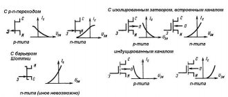
In addition to bipolar transistors, more modern elements - field-effect transistors (Fig. 3.7 - 3.9) have become widespread.
Rice. 3.7. Common source circuit (CS)
Rice. 3.8. Common drain circuit (OS)
By analogy with switching circuits for bipolar transistors, field-effect transistors are switched on with a common source, a common drain, and a common gate.
The main calculated relationships for these circuits for switching field-effect transistors are given in Table 3.4, where S is the slope of the field-effect transistor characteristic, mA/V; R is the internal resistance of the transistor.
Rice. 3.9. Common gate circuit (03)
The main calculated relationships for these circuits for switching field-effect transistors are given in Table 3.4, where S is the slope of the field-effect transistor characteristic, mA/V; R is the internal resistance of the transistor.
The approximate value of R1 (Fig. 3.7 - 3.9) can be from several Ohms to units of MOhm R2 - several kOhms. Note that, as for bipolar transistors, field-effect transistors also allow operation with cutoff and saturation; active and inverse modes.
To increase the current transfer coefficient of a bipolar transistor, “composite” transistors are used, connected according to a Darlington circuit (Fig. 3.10 - 3.13). Their overall gain is somewhat different from the product of the gains of each transistor. At the same time, the temperature stability of the circuit deteriorates.
Rice. 3.10
Rice. 3.11
Rice. 3.12
Rice. 3.13
Literature: Shustov M.A. Practical circuit design (Book 1), 2003