Hello, let's continue our acquaintance with bipolar transistors. In the previous post, a transistor was discussed as an electronic key. But this is not all the capabilities of bipolar transistors; one might even say that the key operating mode is only a small fraction in circuits where transistors are used. In the lion's share of transistor circuits, the transistor is used as an amplification device. In these circuits, the transistor is used in the so-called active region. The transistor, as an amplification device, is included in the amplifier stage, which, in addition to the transistor, also contains power circuits, load and communication circuits with a subsequent stage.
To assemble a radio-electronic device, you can pre-make a DIY KIT kit using the link.
Transistor connection circuits
For bipolar transistors, three connection schemes are possible, which have the ability to amplify power: with a common emitter (CE)
,
common base (OB)
and
common collector (OC)
. The circuits differ in the way they connect the signal source and load (RN).
Common emitter circuit
Scheme with a common base
Circuit with a common collector.
For all transistor switching circuits in the absence of a signal supplied from the source (eG), it is necessary to set the initial mode to direct current
– rest mode. In this case, as mentioned in the previous post, the emitter junction must be open, and the collector junction must be closed. For pnp transistors, this is achieved by applying a negative voltage to the collector (collector voltage E0C) and a negative voltage to the base (bias voltage E0B). For NPN transistors, the polarity of these voltages must be opposite. The rest mode of the transistor is determined by the position of its operating point, which depends on the emitter current IE (almost equal to the collector current IC and depending on E0B) and on the voltage E0C.
Operation of a bipolar transistor.
Let's consider the physical processes occurring during operation of a bipolar transistor. Let's take the NPN model as an example. The principle of operation of a PNP transistor is similar, only the polarity of the voltage between the collector and emitter will be opposite.
As already mentioned in the article about the types of conductivity in semiconductors, a P-type substance contains positively charged ions - holes. N-type substance is saturated with negatively charged electrons. In a transistor, the concentration of electrons in the N region significantly exceeds the concentration of holes in the P region.
Let's connect a voltage source between the collector and emitter VCE (VCE). Under its action, electrons from the upper N part will begin to be attracted to the plus and collect near the collector. However, current will not be able to flow because the electric field of the voltage source does not reach the emitter. This is prevented by a thick layer of collector semiconductor plus a layer of base semiconductor.
Now let's connect the voltage between the base and emitter VBE, but significantly lower than VCE (for silicon transistors the minimum required VBE is 0.6V). Since the layer P is very thin, plus a voltage source connected to the base, it will be able to “reach” with its electric field the N region of the emitter. Under its influence, electrons will be directed to the base. Some of them will begin to fill the holes located there (recombine). The other part will not find a free hole, because the concentration of holes in the base is much lower than the concentration of electrons in the emitter.
As a result, the central layer of the base is enriched with free electrons. Most of them will go towards the collector, since the voltage is much higher there. This is also facilitated by the very small thickness of the central layer. Some part of the electrons, although much smaller, will still flow towards the plus side of the base.
As a result, we get two currents: a small one - from the base to the emitter of the IBE, and a large one - from the collector to the emitter of the ICE.
If you increase the voltage at the base, then even more electrons will accumulate in the P layer. As a result, the base current will increase slightly and the collector current will increase significantly. Thus, with a small change in the base current IB, the collector current IC changes greatly. This is how the signal is amplified in a bipolar transistor . The ratio of the collector current IC to the base current IB is called the current gain. It is designated β, hfe or h21e, depending on the specifics of the calculations carried out with the transistor.
β = IC/IB
Transistor amplification parameters
The amplification properties of transistors for a small alternating signal are assessed using various systems of parameters relating input currents and voltages, but only two main parameters are standardized: h21e and fT (or fh21b). Knowing the parameter of the transistor h21e for a given rest mode IE, you can use the following formulas to determine the main parameters of the amplifier stage in the low-frequency region:
where S is the conductivity of the transistor, re is the emitter resistance of the transistor.
Thus, it is possible to calculate the values of |K|
— transistor voltage gain,
|Ki|
is the transistor current gain,
ZВХ
is the transistor input resistance:
| Amplifier stage parameters | Connection diagram | ||
| OE | ABOUT | OK | |
| |K| | S*RH | S*RH | S*RH /( 1 + S*RH) |
| |Ki| | h21e | h21e/(1 + h21e) | h21e |
| ZВХ | h21e*re | re | h21e*RH |
The areas of application of the amplifier stages OE, OB and OK are determined by their properties.
Common emitter cascade
provides amplification in both voltage and current. Its input impedance is on the order of hundreds of Ohms, and its output impedance is tens of kOhms. A distinctive feature is that it changes the phase of the amplified signal by 180°. It has better amplification properties compared to OB and OK and is therefore the main type of cascade for amplifying small signals.
Cascade with a common base
provides voltage gain only (almost the same as OE). The input resistance of the cascade is (1+h21e) times less than the OE, and the output resistance is (1+h21e) times greater. Unlike the OE, the OB cascade does not change the phase of the amplified signal. The low input impedance of the OB stage limits its use in ULF: in practice it is used only as an element of a differential amplifier.
Cascade with common collector
provides current gain only (almost the same as OE). Unlike the OE cascade, the OK cascade does not change the phase of the amplified signal. At K = 1, the OK cascade seems to repeat the amplified voltage in magnitude and phase. Therefore, such a cascade is called an emitter follower. The input resistance OK depends on the load resistance RH and is large (almost h21e times greater than RH), and the output resistance depends on the resistance of the signal source RG and is small (almost h21e times less than RG). The OK cascade, due to its large input and low output impedance, is used in both preliminary and powerful ULFs.
Amplifier Performance
Since the general emitter connection type is mostly accepted, let's first understand a few important terms related to this connection mode.
Input impedance
Since the input circuit is forward biased, the input impedance will be low. Input resistance is the resistance created by the base-emitter junction to signal flow.
By definition, it is the ratio of a small change in base-emitter voltage (ΔV BE) to the resulting change in base current (ΔI B) at a constant collector-emitter voltage.
Input resistance, Ri= frac DeltaVBE DeltaIB
Where R i = input resistance, V BE = base-emitter voltage and IB = base current.
Output impedance
The output impedance of the transistor amplifier is very high. The collector current changes very little with changes in the collector-emitter voltage.
By definition, it is the ratio of the change in collector-emitter voltage (ΔV CE) to the resulting change in collector current (ΔI C) at a constant base current.
Output impedance = Ro= frac DeltaVCE DeltaIC
Where R o = output resistance, V CE = collector-emitter voltage and IC = collector-emitter voltage.
Effective load on the collector
The load is connected to the collector of the transistor and for a single stage amplifier the output voltage is taken from the collector of the transistor and for a multi stage amplifier the same is collected from the cascaded stages of the transistor circuit.
By definition, it is the total load seen by the AC collector current. In case of single stage amplifiers, the effective collector load is a parallel combination of RC and R o .
Effective collector load, RAC=RC//Ro
= fracRC timesRoRC+Ro=RAC
Therefore, for a single stage amplifier, the effective load is equal to the collector load R C.
In a multistage amplifier (that is, having more than one amplification stage), the input resistance R i of the next stage is also taken into account.
The effective collector load becomes a parallel combination of RC, R o and R i, i.e.
Effective collector load, RAC=RC//Ro//Ri
RC//Ri= fracRCRiRC+Ri
Since the input resistance R i is quite small, hence the effective load is reduced.
Current profit
The current gain when changes in input and output currents are observed is called current gain
. By definition, it is the ratio of the change in collector current (IC) to the change in base current (IB).
Current profit, beta= frac DeltaIC DeltaIB
The value of β ranges from 20 to 500. The current gain indicates that the input current becomes β times the collector current.
Voltage boost
The voltage gain when changes in input and output currents are observed is called voltage gain
. By definition, it is the ratio of the change in output voltage (ΔV CE) to the change in input voltage (ΔV BE).
Voltage gain, AV= frac DeltaVCE DeltaVBE
= frac Change to output current effective load Change to input current input resistance
= frac DeltaIC timesRAC DeltaIB timesRi= frac DeltaIC DeltaIB times fracRACRi= beta times fracRACRi
For one stage R AC = R C.
However, for multi-stage,
RAC= fracRC timesRiRC+Ri
Where R i is the input resistance of the next stage.
Bipolar transistor power circuits
To ensure the specified operating mode of the bipolar transistor, it is necessary to set the position of the quiescent point, determined by the quiescent current IC. For this purpose, two voltages must be applied to the electrodes of the transistor: collector voltage and base mixing voltage. The polarity of these voltages depends on the structure of the transistor. For pnp transistors, both of these voltages must be negative, and for npn - positive, relative to the emitter of the transistor. The values of the collector and base voltages must be different; In addition, the requirements for the stability of these voltages are also different. Therefore, two separate power circuits are used - collector and base.
Bipolar transistor design.
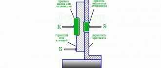
A bipolar transistor consists of three semiconductor layers and two PN junctions. PNP and NPN transistors are distinguished by the type of alternation of hole and electronic conductivity. It's like two diodes connected face to face or vice versa.
A bipolar transistor has three contacts (electrodes). The contact coming out of the central layer is called the base. The outermost electrodes are called collector and emitter. The base layer is very thin relative to the collector and emitter. In addition to this, the semiconductor regions at the edges of the transistor are asymmetrical. The semiconductor layer on the collector side is slightly thicker than on the emitter side. This is necessary for the transistor to operate correctly.
Collector power
Collector power circuits
contain the elements shown below.
In multistage amplifiers, the collector circuits of all stages are connected in parallel to one common source E0C. In this case, the collector power circuit contains an RfSf decoupling filter. The purpose of such a filter is to eliminate parasitic feedback through a common power source. When powered from an alternating current network, the supply voltage ripple is also reduced. Resistor Rф is connected in series with the load RN, and part of the collector voltage is lost on it. Therefore, it is recommended to select resistance Rf based on the permissible voltage drop:
The voltage between the collector and emitter of the UCE transistor is selected within the range
In this case, the minimum value of UC should not be less than 0.5 V, otherwise the operating point goes into the saturation region and nonlinear distortion increases.
Base power circuit diagram
Base power circuits
contains the elements shown below
Fixed current circuit
Fixed voltage circuit
Circuit with automatic bias
The specified operating mode of the transistor is set by applying the required bias voltage UB
or creating the required
bias current IB
. In both cases, a UBE voltage is set between the emitter and the base, equal to (depending on IB) 0.1...0.3 V (for germanium transistors) or 0.5...0.7 V (for silicon ones). The base bias can be carried out from a common power source E0C with the collector or from a separate power source of the base circuits E0B.
When powered by E0C, the base bias can be fixed (current or voltage) or automatic. Fixed Current Circuits
and with
a fixed voltage
do not ensure stability of the transistor operating point when temperature changes.
Modes of operation of the transistor in the amplifier
Before applying a signal to be amplified to the input of a transistor amplifier, it is necessary to ensure the initial operating mode (static mode, direct current mode, rest mode). Initial operating mode
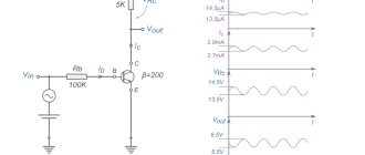
characterized by constant currents of the transistor electrodes and voltages between these electrodes. The term “initial mode of operation of the transistor” and the virtually equivalent term “initial mode of operation of the amplifier” are used. To be specific, let's look at a circuit with a common emitter and the corresponding output characteristics of the transistor. Then the initial operating mode is characterized by the position of the so-called initial operating point (IOP) with coordinates (Uken, Ikn), where Uke and Ikn are the initial voltage between the collector and emitter and the initial collector current. For stable operation of the amplifier, they strive to prevent changes in the position of the initial operating point. To characterize the problem of ensuring the initial regime, the following three schemes are traditionally and quite justifiably considered:
• with fixed base current;
• with collector stabilization;
• with emitter stabilization.
In practice, the first of these schemes is almost never used. Of the other two circuits, preference is often given to the emitter-stabilized circuit. Let's look at each of these schemes.
Circuit with a fixed base current (Fig. 2.14). In such diagrams, the voltage source Ek is usually not depicted.
Rice. 2.14. Circuit with fixed base current
In accordance with Kirchhoff's second law
From here we find the collector current Ik:
which corresponds to a linear relationship of the form:
This equation describes the so-called load line (as for a circuit with a diode). Let us depict the output characteristics of the transistor and the load line (Fig. 2.15).
Rice. 2.15. Transistor output characteristics and load line
In accordance with Kirchhoff's second law
From here we find the base current ib:
We will neglect the voltage ubE, since usually Then i b
Thus, in the circuit under consideration, the current ib is set by the values of Ek and Rb (the current is “fixed”). Wherein
Let ib = ib2. Then the HPT will take the position shown in Fig. 2.15. It is easy to notice that the lowest possible position of the initial operating point corresponds to point Y (cut-off mode, ib = 0), and the highest position corresponds to point Z (saturation mode, ib ib4).
A fixed base current circuit is rarely used for the following reasons:
• under the influence of destabilizing factors (for example, temperature), the values of and change, which changes the current IKN and the position of the initial operating point;
• for each value it is necessary to select the corresponding value of Rb, which is undesirable when using both discrete devices (i.e. devices not manufactured using integrated technology) and integrated circuits.
Scheme with collector stabilization (Fig. 2.16). This scheme provides better stability of the initial mode. The circuit has negative voltage feedback (the output of the circuit - the collector of the transistor is connected to the input of the circuit - the base of the transistor using resistance Rb). Let's consider its manifestation in the following example. Let for some reason (for example, due to an increase in temperature) the current iK began to increase. This will lead to an increase in voltage uRK, a decrease in voltage uke and a decrease in current ib, which will prevent a significant increase in current iK, i.e. The collector current will be stabilized.
Rice. 2.16. Collector stabilization circuit
Circuit with emitter stabilization (Fig. 2.17). In foreign literature, such a circuit is called an H-bias circuit (the circuit configuration corresponds to the letter H).
Rice. 2.17. Emitter-stabilized circuit
The main idea implemented in the circuit is to fix the current iе and through this the current iK (iK iе). For this purpose, a resistor Re is included in the emitter circuit and an almost constant voltage uR E
. It turns out that
To create the required voltage uR e
use a voltage divider across resistors R1 and R2. Resistances R1 and R2 are chosen so small that the current value ib practically does not affect the voltage value uR2. Wherein
In accordance with Kirchhoff's second law
When exposed to destabilizing factors, the value ube changes little, therefore the value uR e
In practice, the voltage
uR e
is usually a small fraction of the voltage Ek.
The following transistor operating modes (operation classes) are distinguished: A, AB, B, C and D. The RC amplifiers under consideration usually operate in mode A. In mode A, the collector current is always greater than zero (iK > 0). At the same time, it increases or decreases depending on the input signal. In mode B IKN = 0, so the collector current can only increase. With a sinusoidal input signal, positive half-waves of current flow in the collector circuit. Mode AB is intermediate between modes A and B. In mode C, an initial blocking voltage is applied to the input of the transistor, so in the collector circuit in each period of the input signal, current flows for a time less than half the period. Mode D is called the key operating mode (the transistor is either in saturation mode or in cutoff mode).