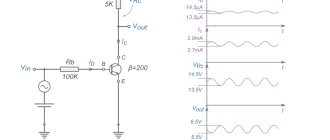
To be specific, let's look at a circuit with a common emitter and the corresponding output characteristics of the transistor. Then the initial operating mode is characterized by the position of the so-called initial operating point (IOP) with coordinates (Uken, Ikn), where Uken and Ikn are the initial voltage between the collector and the emitter and the initial collector current. For stable operation of the amplifier, they strive to prevent changes in the position of the initial operating point.
To characterize the problem of ensuring the initial regime, the following three schemes are traditionally and quite justifiably considered:
- with fixed base current;
- with collector stabilization;
- with emitter stabilization.
Orlov Anatoly Vladimirovich
Head of the Relay Protection and Automation Service of Novgorod Electric Networks
Ask a Question
In practice, the first of these schemes is almost never used. Of the other two circuits, preference is often given to the emitter-stabilized circuit. Let's look at each of these schemes.
Circuit with fixed base current
(Fig. 2.14).
In such diagrams, the voltage source Ek is usually not depicted.
In accordance with Kirchhoff's second law ik · Rk + uke− Ek = 0 From here we find the collector current ik: ik= − ( 1 / Rk ) · uke+ ( 1 / Rk ) · Ek which corresponds to a linear dependence of the form y = a · x + b. This equation describes the so-called load line (as for a circuit with a diode).
Let us depict the output characteristics of the transistor and the load line (Fig. 2.15).
In accordance with Kirchhoff’s second law, ib · Rb + ube − Ek = 0
From here we find the base current ib: ib = − ube / Rb + Ek / Rb
We will neglect the voltage ube since usually ube << Ek. Then ib = Ek / Rb
Thus, in the circuit under consideration, the current ib is set by the values of Ek and Rb (the current is “fixed”). In this case, ik= βst · ib + Íko
Let ib = ib2. Then the HPT will take the position shown in Fig. 2.15. It is easy to notice that the lowest possible position of the initial operating point corresponds to point Y (cut-off mode, ib = 0), and the highest position corresponds to point Z (saturation mode, ib > ib4).
A fixed base current circuit is rarely used for the following reasons:
- when exposed to destabilizing factors (for example, temperature), the values of βst and Íko change, which changes the current Ikn and the position of the initial operating point.
- for each value of βst, it is necessary to select the corresponding value of Rb, which is undesirable when using both discrete devices (i.e., devices not manufactured using integrated technology) and integrated circuits.
Static modes of switches on bipolar transistors
( 2 )
The saturation depth of the transistor (saturation coefficient s) is characterized by the ratio of the real current Ib to the minimum base current required for saturation:
( 3 )
From (1) and (2) we can determine the minimum voltage Uin that is required for saturation by setting Ib = Ibn:
( 4 )
When a load is connected to the switch output, the static output voltage levels change. In digital circuits, a switch typically loads the input circuit of another switch of the same type (or several identical keys), as shown in Fig. 4. Such a load has virtually no effect on the saturated transistor mode, since the inputs of the external switches have a potential almost equal to zero, the transistors of the external switches are closed, there is no input current in them, and there is also no component of the load current in the analyzed switch.
The load connected according to the diagram in Fig. 4 affects the closed mode of the transistor. In this case, the output of the analyzed key has a high voltage level - the foreign keys are open. The external load circuit can be replaced with an equivalent load resistor Rн connected between the collector and emitter of a closed transistor. The load current (flowing from the switch), which flows through the resistor Rk, lowers the output voltage level in the analyzed switch. It is now equal
( 5 )
Integrated logic elements that use bipolar saturated transistors are characterized by a switch (inverter) circuit with a control (switching) input transistor (Fig. 2). In TTL elements, to expand the logical capabilities, the input transistor T1 is made multi-emitter (in this case, the circuit implements the logical AND-NOT operation).
The control voltage in the switch Fig. 2 is unipolar (positive). Provided that the voltage is the output voltage of another switch of the same type, it can vary from to In the switch of Fig. 2, in contrast to the key of Fig. 1, the currents of the output transistor T2 in static states are practically independent of voltage.
When transistor T1 is in a saturated state, because both of its junctions are biased in the forward direction (the base potential of transistor T1 is higher than the potential of its emitter and collector, because , a ). For a saturated transistor T1 we have, then <, so transistor T2 is closed and there is no base current for transistor T2. The flowing current is closed through the control voltage source and is set by a resistor:
Go to page: 2
Other on the topic:
Design of a digital radio relay line One of the main types of modern communications are line-of-sight radio relay lines (RLL), which are used to transmit signals of multi-channel telephone messages, radio broadcasting and television, telegraph and phototelegraph signals, ...
Collector stabilization circuit
(Fig. 2.16).
Vasiliev Dmitry Petrovich
Professor of Electrical Engineering, St. Petersburg State Polytechnic University
Ask a Question
This scheme provides better stability of the initial mode. The circuit has negative voltage feedback (the output of the circuit - the collector of the transistor is connected to the input of the circuit - the base of the transistor using resistance Rb.). Let's consider its manifestation in the following example.
Let for some reason (for example, due to an increase in temperature) the current ik began to increase. This will lead to an increase in voltage uRk, a decrease in voltage uke and a decrease in current ib (ib = uke/Rb), which will prevent a significant increase in current iк, i.e. the collector current will be stabilized.
Emitter-stabilized circuit
In foreign literature, such a circuit is called an H-bias circuit (the configuration of the circuit corresponds to the letter H). The main idea implemented in the circuit is to fix the current iе and through this the current ik (ik = iе). For this purpose, a resistor Re is connected to the emitter circuit and an almost constant voltage uRe is created across it. It turns out that iе= uRe/ Re= const. To create the required voltage uR, a voltage divider is used across resistors R1 and R2. Resistances R1 and R2 are chosen so small that the current value ib practically does not affect the voltage value uR2. In this case, uR2= Eк · [ R2/ ( R1+ R2)] In accordance with Kirchhoff’s second law uRe= uR2– ub
When exposed to destabilizing factors, the value ube changes little, therefore the value uRe changes little. In practice, the voltage uRe is usually a small fraction of the voltage Ek.
The following transistor operating modes (operation classes) are distinguished: A, AB, B, C and D.
The RC amplifiers under consideration usually operate in mode A.
- In mode “A” the collector current is always greater than zero (ik > 0). At the same time, it increases or decreases depending on the input signal.
- In mode “B” Icl = 0, so the collector current can only increase. With a sinusoidal input signal, positive half-waves of current flow in the collector circuit.
- Mode "AB" is intermediate between modes A and B.
- In mode “C”, an initial blocking voltage is applied to the input of the transistor, so in the collector circuit in each period of the input signal, current flows for a time less than half the period.
- Mode “D” is called the key operating mode (the transistor is either in saturation mode or in cutoff mode).
Bipolar transistor structure
Transistors are divided into two main classes: bipolar and field-effect.
Bipolar transistor
is a semiconductor device with two interacting electrical junctions and three (or more) terminals, the amplifying properties of which are determined by the phenomena of injection and extraction of minority charge carriers.
There are two types of bipolar transistors: drift-free (diffusion) and drift - they differ in their operating principle. Let's consider drift-free bipolar transistors.
Structurally, a bipolar transistor is a semiconductor single crystal plate with p- or n-type electrical conductivity, on both sides of which semiconductors having a different type of electrical conductivity are fused (or introduced in another way). At the interface between regions with different types of electrical conductivity, pn- or np-junctions are formed. Each of the regions, called emitter 1, collector 2 and base 3, is supplied with an ohmic contact from which E, K and B are drawn, respectively (Fig. 1.25). Bipolar transistor base
– the middle region in the pnp- (or npn-) structure, characterized by the lowest concentration of impurities, is connected through an ohmic contact to a terminal called the base (B).
The emitter
is the outermost region in the pnp (or npn) structure of a bipolar transistor, used for injecting carriers into the base region, connected through an ohmic contact to a terminal called the emitter (E).
Collector
- the outermost region in the pnp- (or npn-) structure of
a bipolar transistor
, used to extract (pull in) carriers from the base region; through an ohmic contact it is connected to a terminal called the collector (K). The transistor is mounted on a crystal holder and placed in a sealed housing, into the bottom of which leads pass through glass insulators. The body can be metal, plastic or glass.
Rice. 1.25. Bipolar transistor
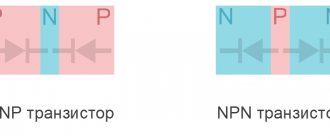
When considering the processes occurring in a transistor, it is convenient to represent it in planar block diagrams. Shown in Fig. 1.25 transistor in the form of a block diagram is shown in Fig. 1.26, a. It has a pn-p structure. In Fig. 1.26, b shows a transistor with a different alternation of areas (npn), in Fig. 1.26, c, d – symbols of transistors corresponding to block diagrams. There is no difference in the principle of operation of the transistors of both structures, but the polarity of connecting the terminals to the power source is opposite. Since the transistor is a symmetrical structure, any extreme region could be both an emitter and a collector. However, in real designs, in order to ensure better operation of the transistor, the collector area is made larger in size than the emitter area. For the same reasons, the active thickness of the base is made small (less than the diffusion length of minority carriers). The pins from each of the areas are called the same as the areas: emitter, base, collector. The emitter-base junction is called emitter, and the collector-base junction is called collector. The purpose of the emitter is injection (injection) into the base area of charge carriers that are not the main ones for it, for which the emitter area is made more saturated with the main carriers (lower resistance) than the base area. The purpose of the collector is the extraction (retraction) of carriers from the base, in which three areas are distinguished: active (between the emitter and collector, through which charge carriers arrive in the active mode of operation of the transistor), passive (between the emitter and the base output) and peripheral (behind base output).
Transistors are classified according to various criteria: by power - low, medium, high; by operating frequency range - low, medium, high; by manufacturing method - alloy, microalloy, diffusion, planar, mesastructures.
Rice. 1.26. Planar block diagrams and symbols of transistors
- Back
- Forward
