Bipolar transistor - an electronic semiconductor device, one of the types of transistors, designed to amplify, generate and convert electrical signals. The transistor is called bipolar because two types of charge carriers - electrons and holes - are simultaneously involved in the operation of the device. This differs from a unipolar (field-effect) transistor, in which only one type of charge carrier is involved.
The principle of operation of both types of transistors is similar to the operation of a water tap that regulates the flow of water, only a flow of electrons passes through the transistor. In bipolar transistors, two currents pass through the device - the main “large” current, and the control “small” current. The main current power depends on the control power. With field-effect transistors, only one current passes through the device, the power of which depends on the electromagnetic field. In this article we will take a closer look at the operation of a bipolar transistor.
Bipolar transistor design.
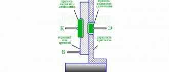
A bipolar transistor consists of three semiconductor layers and two PN junctions. PNP and NPN transistors are distinguished by the type of alternation of hole and electronic conductivity. It's like two diodes connected face to face or vice versa.
A bipolar transistor has three contacts (electrodes). The contact coming out of the central layer is called the base. The outermost electrodes are called collector and emitter. The base layer is very thin relative to the collector and emitter. In addition to this, the semiconductor regions at the edges of the transistor are asymmetrical. The semiconductor layer on the collector side is slightly thicker than on the emitter side. This is necessary for the transistor to operate correctly.
Operation of a bipolar transistor.
Let's consider the physical processes occurring during operation of a bipolar transistor. Let's take the NPN model as an example. The principle of operation of a PNP transistor is similar, only the polarity of the voltage between the collector and emitter will be opposite.
As already mentioned in the article about the types of conductivity in semiconductors, a P-type substance contains positively charged ions - holes. N-type substance is saturated with negatively charged electrons. In a transistor, the concentration of electrons in the N region significantly exceeds the concentration of holes in the P region.
Let's connect a voltage source between the collector and emitter VCE (VCE). Under its action, electrons from the upper N part will begin to be attracted to the plus and collect near the collector. However, current will not be able to flow because the electric field of the voltage source does not reach the emitter. This is prevented by a thick layer of collector semiconductor plus a layer of base semiconductor.
Now let's connect the voltage between the base and emitter VBE, but significantly lower than VCE (for silicon transistors the minimum required VBE is 0.6V). Since the layer P is very thin, plus a voltage source connected to the base, it will be able to “reach” with its electric field the N region of the emitter. Under its influence, electrons will be directed to the base. Some of them will begin to fill the holes located there (recombine). The other part will not find a free hole, because the concentration of holes in the base is much lower than the concentration of electrons in the emitter.
As a result, the central layer of the base is enriched with free electrons. Most of them will go towards the collector, since the voltage is much higher there. This is also facilitated by the very small thickness of the central layer. Some part of the electrons, although much smaller, will still flow towards the plus side of the base.
As a result, we get two currents: a small one - from the base to the emitter of the IBE, and a large one - from the collector to the emitter of the ICE.
If you increase the voltage at the base, then even more electrons will accumulate in the P layer. As a result, the base current will increase slightly and the collector current will increase significantly. Thus, with a small change in the base current IB, the collector current IC changes greatly. This is how the signal is amplified in a bipolar transistor . The ratio of the collector current IC to the base current IB is called the current gain. It is designated β, hfe or h21e, depending on the specifics of the calculations carried out with the transistor.
β = IC/IB
Physical processes
Let's take an npn type transistor in no-load mode, when only two sources of constant supply voltages E1 and E2 are connected. At the emitter junction the voltage is forward, at the collector junction it is reverse. Accordingly, the resistance of the emitter junction is low and a voltage of tenths of a volt E1 is sufficient to obtain a normal current. The collector junction resistance is high and the voltage E2 is usually tens of volts.
Accordingly, as before, dark small circles with arrows are electrons, red ones are holes, large circles are positively and negatively charged atoms of donors and acceptors. The current-voltage characteristic of the emitter junction is the characteristic of a semiconductor diode with forward current, and the current-voltage characteristic of the collector junction is similar to the current-voltage characteristic of the diode with reverse current.
The principle of operation of the transistor is as follows. The forward voltage of the emitter junction uub-e affects the emitter and collector currents and the higher it is, the greater these currents. The changes in the collector current are only slightly less than the changes in the emitter current. It turns out that the voltage at the base-emitter junction, i.e., the input voltage, controls the collector current. This phenomenon is based on the amplification of electrical oscillations using a transistor. The main bipolar transistors are shown in the table below.
Table of characteristics of bipolar transistors.
As the forward input voltage uub-e increases, the potential barrier in the emitter junction decreases and, accordingly, the current through this junction ie increases. Electrons of this current are injected from the emitter into the base and, due to diffusion, penetrate through the base into the collector junction, increasing the collector current. Since the collector junction operates at a reverse voltage, space charges arise in this junction (large circles in the figure). An electric field arises between them, which promotes the movement (extraction) through the collector junction of electrons that came here from the emitter, i.e., they draw electrons into the region of the collector junction.
Scheme of operation and design of a bipolar transistor.
If the thickness of the base is small enough and the concentration of holes in it is low, then most of the electrons, having passed through the base, do not have time to recombine with the holes of the base and reach the collector junction. Only a small fraction of the electrons recombine with holes in the base. As a result, a base current arises.
Current base is useless and even harmful. It is desirable that it be as small as possible. That is why the base area is made very thin and the concentration of holes in it is reduced. Then fewer electrons will recombine with holes and, again, the base current will be insignificant.
When no voltage is applied to the emitter junction, we can assume that there is no current in that junction. Then the region of the collector junction has a significant resistance to direct current, since the main charge carriers move away from this junction and regions depleted of these carriers are created along both boundaries. Very little reverse current flows through the collector junction, caused by minority carriers moving towards each other.
It will be interesting➡ Types and design of optocouplers (optocouplers)
If, under the influence of the input voltage, a significant emitter current arises, then electrons are injected into the base from the emitter side, which for this region are minority carriers. They reach the collector junction without having time to recombine with holes when passing through the base.
The higher the emitter current, the more electrons come to the collector, the lower its resistance becomes, therefore, the collector current increases. Similar phenomena occur in a pnp transistor, you just need to change the positions of the electrons and holes, as well as the polarity of the sources E1 and E2.
How does a transistor work?
In addition to the processes considered, there are a number of other phenomena. Let us consider the modulation of the base thickness. When the voltage at the collector junction increases, avalanche charge multiplication occurs in it, mainly due to impact ionization.
This phenomenon and the tunneling effect can cause electrical breakdown, which can turn into thermal breakdown as the current increases. Everything happens the same as with diodes, but in a transistor with excessive collector current, thermal breakdown can occur without prior electrical breakdown.
Thermal breakdown can occur without increasing the collector voltage to breakdown voltage. When the voltages on the collector and emitter junctions change, their thickness changes, resulting in a change in the thickness of the base.
It is especially important to take into account the collector-base voltage, since in this case the thickness of the collector increases, the thickness of the base decreases. With a very thin base, a closing effect may occur (the so-called “puncture” of the base) - a connection between the collector junction and the emitter junction. In this case, the base area disappears and the transistor stops working normally.
As the injection of carriers from the emitter into the base increases, minority charge carriers accumulate in the base, i.e., the concentration and total charge of these carriers increases. But when the injection decreases, the concentration and total charge of these same carriers in the base decreases, and this process is called the resorption of minority charge carriers in the base.
And finally, one rule: when operating transistors, it is prohibited to break the base circuit unless the power to the collector circuit is turned on. It is also necessary to turn on the power to the base circuit, and then to the collector circuit, but not vice versa.
Transistor circuit diagram.
Bipolar transistors
A bipolar transistor is a semiconductor device consisting of three alternating regions of a semiconductor with different types of conductivity (p-p-p or p-p-p) with a terminal from each region. Let's consider the operation of an n-p-n-type transistor. The alternating regions form two pn junctions, base–emitter (BE) and base–collector (BC).
A direct voltage EBE is applied to the BE junction, under the influence of which electrons from the n-region of the emitter rush to the base, creating an emitter current. The concentration of impurities in the emitter is many times greater than in the base, and the base itself is as thin as possible. Therefore, only a small fraction (1–5%) of the electrons emitted by the emitter recombine with holes in the base.
Most of the electrons, having passed the narrow (fractions of a micron) region of the base, are “collected” by the collector voltage Ek, which represents the reverse voltage for the BC junction, and, rushing to the plus of the external source Ek, creates a collector current flowing through the load Rн. Electrons that have recombined with holes in the base make up the base current IB.
The collector current is thus determined by the emitter current minus the base current. A pnp-type transistor works similarly, differing only in that its emitter emits holes, not electrons, into the base, therefore the polarities of the direct UEB and reverse Ek voltages applied to it must be opposite to the pnp-type transistor.
Important on the topic. How to ring a transistor.
On the symbol of transistors, the arrow is placed on the emitter and is always directed from the p-region to the n-region. In Fig. 1.8, b shows the symbol of the transistor p-p-p, and in Fig. 1.9, b – p-p-p. A circle around the transistor means that the transistor is manufactured in a separate package, and the absence of a circle means that the transistor is made integral with other elements on the semiconductor plate of the integrated circuit.
It will be interesting➡ Marking of different types of diodes
It is convenient to think of the emitter arrow as an indicator of the polarity of the forward voltage applied between the base and emitter, which “opens” (like a rectifier diode) the transistor. When using a transistor in electronic devices, two terminals are needed for the input signal and two for the output signal.
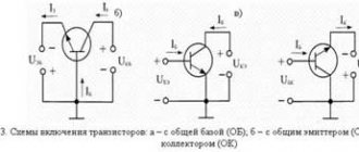
Since the transistor has only three terminals, one of them must be common, belonging simultaneously to both the input and output circuits. Three options for transistor connection circuits are possible - with a common base, a common emitter and a common collector.
Transition in a bipolar transistor.
Scheme with a common base
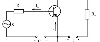
The circuit diagram for connecting a transistor with a common base (CB) is shown in Fig. 1.10. The input signal for the circuit with OB is the voltage applied between the emitter and the base UBX = = UEB; output – voltage released at the load Uout = IкRн; input current – emitter current Iin = IE; output current – collector current Iout = Iк.
The input voltage UEB is the control voltage for the transistor, so a small change in it (a fraction of a volt) leads to a change in the emitter current over a very wide range - practically from zero to maximum. The maximum current is determined by the purpose of the transistor (low power, medium power and high power) and the corresponding design.
Since the voltage UΚB is reverse, the value of the external source voltage Ek can be tens of times higher than the value of the voltage UEB. The greater the collector current, the greater the voltage drop across the load, while only a small voltage UKB will drop across the transistor itself, which will be smaller the greater the collector current.
Thus, a change of a fraction of a volt in the input voltage leads to a change in the voltage at the load, slightly less than the voltage Ek. This position determines the amplifying properties of the transistor.
To evaluate the operation of the transistor and its amplifying properties in various switching circuits, the increments of input values and the resulting increments of output values are considered. Considering a transistor as an amplifier, it is customary to characterize its properties by the gain factors and the value of the input resistance. There are three types of gain factors:
- • current gain KI = ΔIout /ΔIin;
- • voltage gain КU = ΔUout/ΔUin;
- • power gain KR = KI • KU.
The ratio of the change in input voltage to the change in input current: Rin = ΔUin/ΔIin. The input impedance of any amplifier leads to distortion of the input signal. Any real signal source has some internal resistance, and when it is connected to an amplifier, a voltage divider is formed, consisting of the internal resistance of the source and the input resistance of the amplifier.
Therefore, the higher the input impedance of the amplifier, the larger part of the signal will be released at this resistance and amplified, and the smaller part of it will fall at the internal resistance of the source itself. Thus, the BDC is also determined by the resistance ratio. Since the gain of the circuit with OB for current KIB turns out to be less than unity, it has not found application.
Bipolar transistor dimensions.
The simplest bipolar transistor amplifier
Let us consider in more detail the principle of signal amplification in the electrical plane using the example of a circuit. Let me make a reservation in advance that this scheme is not entirely correct. No one connects a DC voltage source directly to an AC source. But in this case, it will be easier and more clear to understand the amplification mechanism itself using a bipolar transistor. Also, the calculation technique itself in the example below is somewhat simplified.
1.Description of the main elements of the circuit
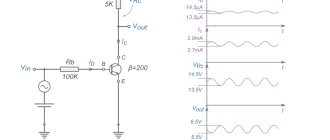
So, let’s say we have a transistor with a gain of 200 (β = 200). On the collector side, we will connect a relatively powerful 20V power source, due to the energy of which amplification will occur. From the base of the transistor we connect a weak 2V power source. We will connect to it in series an alternating voltage source in the form of a sine wave, with an oscillation amplitude of 0.1V. This will be a signal that needs to be amplified. The resistor Rb near the base is necessary in order to limit the current coming from the signal source, which usually has low power.
Calculation of base input current Ib
Now let's calculate the base current Ib. Since we are dealing with alternating voltage, we need to calculate two current values - at the maximum voltage (Vmax) and minimum (Vmin). Let's call these current values Ibmax and Ibmin, respectively.
Also, in order to calculate the base current, you need to know the base-emitter voltage VBE. There is one PN junction between the base and emitter. It turns out that the base current “meets” the semiconductor diode on its path. The voltage at which a semiconductor diode begins to conduct is about 0.6V. We will not go into details of the current-voltage characteristics of the diode, and for simplicity of calculations we will take an approximate model, according to which the voltage on the current-carrying diode is always 0.6V. This means that the voltage between base and emitter VBE = 0.6V. And since the emitter is connected to ground (VE = 0), the voltage from base to ground is also 0.6V (VB = 0.6V).
Let's calculate Ibmax and Ibmin using Ohm's law:
Calculation of collector output current IC
Now, knowing the gain (β = 200), you can easily calculate the maximum and minimum values of the collector current (Icmax and Icmin).
Calculation of output voltage Vout
It remains to calculate the voltage at the output of our amplifier Vout. In this circuit, this is the voltage at the collector VC.
The collector current flows through the resistor Rc, which we have already calculated. It remains to substitute the values:
Analysis of results
As can be seen from the results, VCmax turned out to be less than VCmin. This is because the voltage across resistor VRc is subtracted from the supply voltage VCC. However, in most cases this does not matter, since we are interested in the variable component of the signal - the amplitude, which has increased from 0.1V to 1V. The frequency and sinusoidal shape of the signal have not changed. Of course, a Vout/Vin ratio of ten times is far from the best indicator for an amplifier, but it is quite suitable for illustrating the amplification process.
So, let's summarize the principle of operation of an amplifier based on a bipolar transistor. A current Ib flows through the base, carrying DC and AC components. A constant component is needed so that the PN junction between the base and emitter begins to conduct - “opens”. The variable component is, in fact, the signal itself (useful information). The collector-emitter current inside the transistor is the result of the base current multiplied by the gain β. In turn, the voltage across the resistor Rc above the collector is the result of multiplying the amplified collector current by the resistor value.
Thus, the Vout pin receives a signal with an increased oscillation amplitude, but with the same shape and frequency. It is important to emphasize that the transistor takes energy for amplification from the VCC power source. If the supply voltage is insufficient, the transistor will not be able to operate fully, and the output signal may be distorted.
Physical equivalent circuits of bipolar transistors
As already mentioned, physical equivalent circuits are built on the basis of a one-dimensional theoretical model, which assumes that physical processes in semiconductor structures can be considered localized in certain areas and taken into account by including a certain (finite) number of elements (resistors, capacitors, current sources, etc.) in equivalent circuits. P.).Physical equivalent circuits, as well as equivalent circuits of pass-through linear quadripoles, can be built for various transistor circuits. However, since the switching circuit itself cannot affect the physical characteristics of the transistor, almost all parameters of the physical equivalent circuits remain the same regardless of the transistor's switching circuit.
In Fig. 4.13, 4.14 present the two simplest ways to construct physical equivalent circuits of a bipolar transistor. In the diagram in Fig. 4.13, the amplifying properties of the transistor are modeled by including an idealized current source in the collector circuit, and in the circuit in Fig. 4.14 - voltage source. In addition, in both cases different groups of physical parameters can be used for the elements of the equivalent circuit.
Rice. 4.13. T-shaped small-signal physical equivalent circuit of a \(p\)-\(n\)-\(p\)-type bipolar transistor with a current source
Rice. 4.14. T-shaped small-signal physical equivalent circuit of a \(n\)-\(p\)-\(n\)-type bipolar transistor with a voltage source
All quantities that act as parameters of elements of physical equivalent circuits have a clear physical meaning:
- \(r_b\) - differential resistance of the base region of the transistor, equal to the sum of the distributed resistance of the base \(r_b^{\prime}\) and its diffusion resistance \(r_b^{"}\): \(r_b = r_b^{\prime } + r_b^{"}\), typical for low-power planar transistors are the values \(r_b \approx {10...100 Ohm}\);
- \(r_e\) is the differential resistance of the emitter, in practice it is often observed:
\(r_e = r_E \approx \cfrac{0.025}{{I_E}_0}\);
- \(r_к\) is the differential resistance of the collector in a circuit with OB, usually this resistance is much greater than \(r_е\) and \(r_b\) and amounts to tens or hundreds of kilo-ohms;
- \(C_к\) is the capacitance of the collector junction in the circuit with OB;
- \(\alpha\) is the differential transfer coefficient of the emitter current in the circuit with OB;
- \(\beta\) - differential base current transfer coefficient in a circuit with OE,
\( \beta \approx \cfrac{\alpha}{\left( 1 — \alpha \right)} \);
- \(r_к^*\) - differential resistance of the collector in a circuit with OE,
\( r_к^* \approx \cfrac{r_к}{\left( \beta + 1 \right)} \);
- \(C_к^*\) is the capacitance of the collector junction in a circuit with OE,
\( C_к^* \approx C_к \left( \beta + 1 \right) \);
- \(r_r\) - resistance, reflecting the amplifying properties of the transistor in a circuit with OB,
\(r_r = \alpha r_k\);
- \(r_r^*\) - resistance, reflecting the amplifying properties of the transistor in a circuit with OE,
\(r_r^* = \beta r_k^*\).
When depicting physical equivalent circuits, they try to take the positive directions of alternating currents and voltages to coincide with real direct currents and voltages at the corresponding electrodes of the transistor (complete coincidence is usually not achieved).
In the case of considering any specific circuit for switching on a bipolar transistor, one of its electrodes is common to the input and output of the circuit, and the choice of the option (with a current source or with a voltage source) of the equivalent circuit is made taking into account the convenience of calculations and analysis of the model.
Somewhat less obvious is the choice of one or another group of parameters of the elements of the equivalent circuit (see options 1, 2 in Fig. 4.13, 4.14). Here, first of all, you need to be guided by the circuit for connecting the transistor to the amplifier stage. If this is a circuit with OE, then it is always better to use option 1 (according to Fig. 4.13, 4.14), in a circuit with OB - option 2, but for a circuit with OK, both the first (in most cases) and second options may be convenient , depending on what properties of the circuit we are analyzing and in what mode the transistor operates (by mode here we mean the entire set of external influences exerted on the device).
In general, the differences between the parameters of the equivalent circuit for different methods of connecting a transistor to an amplifier stage are dictated primarily by some inaccuracy of the constructed model of physical processes in the transistor. Those. We are trying to increase the accuracy of this model by adjusting the parameters of some elements of the equivalent circuit, taking into account the characteristics of the transistor for each specific way of turning it on. It should be understood that in this way (by choosing the correct version of the parameters used in Fig. 4.13, 4.14) we can only slightly increase the accuracy of the analysis, but not achieve any radically new results.
As a specific example in Fig. Figure 4.15 shows the equivalent circuit of a bipolar transistor in connection with an OB (version with a current generator \(\alpha \dot{I}_E\)), it is precisely this circuit that we will use in the future to analyze the amplification stages on transistors in connection with an OB.
Rice. 4.15. T-shaped small-signal physical equivalent circuit of a bipolar transistor \(n\)-\(p\)-\(n\)-type with a current source \(\alpha .I_e\) when switched on with OB
The capacitances shown in the equivalent circuits with dotted lines (Fig. 4.13, 4.14, 4.15) make it possible to simulate the manifestation of reactivity in the transistor as the frequency of the alternating signal increases. As can be seen from equivalent circuits, they are usually limited to considering only the collector junction capacitance of a bipolar transistor, which, as a rule, is higher than all other available capacitances and has the greatest impact on the amplifying properties of the transistor. However, in the general case, when performing high-frequency analysis, one should not only add the capacitance of the collector junction, but also take into account the frequency dependences of the parameters of other elements of the physical equivalent circuit of the transistor (primarily the transmission coefficients \(\alpha\) and \(\beta\)).
An example of a high-frequency physical equivalent circuit of a bipolar transistor connected with an OB, where the frequency dependence of the emitter current transfer coefficient \(\alpha(\omega)\) is modeled by an additional \(RC\)-chain, is shown in Fig. 4.16. In this scheme, the values of \(R\) and \(C\) are selected based on the relationship.
Rice. 4.16. Small-signal high-frequency physical equivalent circuit of a \(n\)-\(p\)-\(n\)-type bipolar transistor
After a series of successive simplifications, this scheme is reduced to the form shown in Fig. 4.17 (the so-called Pritchard scheme). A significant advantage of such a scheme is that its elements have a very definite physical meaning.
Rice. 4.17. Simplified small-signal high-frequency physical equivalent circuit of a \(n\)-\(p\)-\(n\)-type bipolar transistor (Pritchard circuit)
The parameters of physical equivalent circuits can be expressed through the differential parameters of a four-terminal transistor (Table 4.5). You just need to understand that such formulas are correct only with a certain accuracy, since there are some differences between the physical models of transistors and the model of a linear pass-through four-terminal network.
Tab. 4.5. Relationship between the physical parameters of a bipolar transistor and its differential \(h\)-parameters
| Next > |
Operating modes of a bipolar transistor
In accordance with the voltage levels on the electrodes of the transistor, there are four modes of its operation:
- Cut off mode.
- Active mode.
- Saturation mode.
- Inverse mode (reverse mode).
Cut-off mode
When the base-emitter voltage is lower than 0.6V - 0.7V, the PN junction between the base and emitter is closed. In this state, the transistor has no base current. As a result, there will be no collector current either, since there are no free electrons in the base ready to move towards the collector voltage. It turns out that the transistor is, as it were, locked, and they say that it is in cutoff mode.
Active mode
In active mode, the voltage at the base is sufficient for the PN junction between the base and emitter to open. In this state, the transistor has base and collector currents. The collector current equals the base current multiplied by the gain. That is, the active mode is the normal operating mode of the transistor, which is used for amplification.
Saturation mode
Sometimes the base current may be too high. As a result, the supply power is simply not enough to provide such a magnitude of collector current that would correspond to the gain of the transistor. In saturation mode, the collector current will be the maximum that the power supply can provide and will not depend on the base current. In this state, the transistor is not able to amplify the signal, since the collector current does not respond to changes in the base current.
In saturation mode, the conductivity of the transistor is maximum, and it is more suitable for the function of a switch (switch) in the “on” state. Similarly, in the cut-off mode, the conductivity of the transistor is minimal, and this corresponds to the switch in the off state.
Inverse mode
In this mode, the collector and emitter change roles: the collector PN junction is biased in the forward direction, and the emitter junction is biased in the opposite direction. As a result, current flows from the base to the collector. The collector semiconductor region is asymmetrical to the emitter, and the gain in inverse mode is lower than in normal active mode. The transistor is designed in such a way that it operates as efficiently as possible in active mode. Therefore, the transistor is practically not used in inverse mode.
Transistor operating principle
In the active operating mode, the transistor is turned on so that its emitter junction is biased in the forward direction (open), and the collector junction is biased in the opposite direction. For definiteness, let’s consider an npn transistor; all reasoning is repeated in exactly the same way for the case of a pnp transistor, with the word “electrons” replaced by “holes”, and vice versa, as well as with all voltages replaced with opposite signs.
In an NPN transistor, electrons, the majority current carriers in the emitter, pass through an open emitter-base junction into the base region. Some of these electrons recombine with the majority charge carriers in the base (holes), while some diffuse back into the emitter.
However, because the base is made very thin and very lightly doped, most of the electrons injected from the emitter diffuse into the collector region. The strong electric field of a reverse-biased collector junction captures electrons (recall that they are minority carriers in the base, so the junction is open for them) and carries them into the collector. The collector current is thus practically equal to the emitter current, with the exception of a small recombination loss in the base, which forms the base current (Ie = Ib + Ik).
The coefficient α connecting the emitter current and the collector current (Iк=α Iе) is called the emitter current transfer coefficient. The numerical value of the coefficient α is 0.9 - 0.999, the higher the coefficient, the better the transistor. This coefficient depends little on the collector-base and base-emitter voltages.
Over a wide range of operating voltages, the collector current is proportional to the base current, the proportionality coefficient is β=α/(1-α)=(10-1000). That. By changing the small base current, you can control a much larger collector current.
Bipolar transistor is an electrical converting semiconductor device with one or more electrical junctions, designed to amplify, convert and generate electrical signals. The entire structure is performed on a wafer of silicon, or germanium, or other semiconductor, in which three regions with different types of electrical conductivity are created.
It will be interesting➡ What is a varicap?
The middle region is called the base, one of the outer regions is the emitter, and the other is the collector. Accordingly, the transistor has two pn junctions: the emitter - between the base and the emitter and the collector - between the base and the collector.
The base area must be very thin, much thinner than the emitter and collector areas (this is shown disproportionately in the figure). The condition for good operation of the transistor depends on this. The transistor operates in three modes depending on the voltage at its junctions.
When operating in active mode, the voltage at the emitter junction is direct, and at the collector junction it is reverse. In cutoff mode, reverse voltage is applied to both junctions. If direct voltage is applied to these junctions, the transistor will operate in saturation mode.
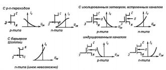
Types of bipolar transistors.