Classification of field effect transistors
Let's start with the classification. There are numerous types of field-effect transistors, each working according to an algorithm:
- Channel conductivity type: n or p. The factor determines the polarity of the control voltage.
- By structure. With p-n junction alloy, diffusion, MIS (MOS), with Schottky barrier, thin film.
- The number of electrodes is 3 or 4. In the latter case, the substrate is considered a separate entity, allowing you to control the flow of current through the channel (in addition to the gate).
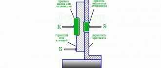
- Conductor material. Today, silicon, germanium, and gallium arsenide are common. The semiconductor material is marked with a symbol such as letters (K, G, A) or (in military industry products) numbers (1, 2, 3).
- The application class is not included in the marking; it is indicated by reference books that provide information that the field-effect transistor is often included in amplifiers and radio receivers.
In world practice, there is a division according to applicability into the following 5 groups: high-frequency, low-frequency, direct current amplifiers, modulators, key ones. Semiconductor transistor - The range of electrical parameters determines the set of values in which the field-effect transistor remains operational. Voltage, current, frequency.
- Based on their design features, they are divided into unitrons, alkatrons, teknetrons, and gridistors. Each device is equipped with key features. Alkatron electrodes are made of concentric rings, increasing the volume of current passed.
- Based on the number of structural elements contained in one substrate, they are classified as double, complementary.
In addition to the general classification, a specialized one has been invented that defines the principles of operation. There are:
- Field-effect transistors with control pn junction.
- Field effect transistors with a Schottky barrier.
- Insulated gate field effect transistors:
- With built-in channel.
- With induced channel.
In the literature, structures are further ordered as follows: it is not practical to use the MOS designation; oxide structures are considered a special case of MOS (metal, dielectric, semiconductor). The Schottky barrier (MeP) should be highlighted separately, since it is a different structure. Reminds the properties of a pn junction. Let us add that, structurally, the transistor can simultaneously contain a dielectric (silicon nitride) and an oxide (tetravalent silicon), as happened with KP305. Such technical solutions are used by people looking for methods to obtain unique properties of a product and reduce the cost.
FET devices
Among foreign abbreviations for field-effect transistors, the combination FET is reserved, sometimes denoting the type of control - with a pn junction. In the latter case, we will also encounter JFET. Synonymous words. Abroad, it is customary to separate oxide (MOSFET, MOS, MOST - synonyms), nitride (MNS, MNSFET) field-effect transistors. The presence of a Schottky barrier is marked by SBGT. Apparently, the material is significant, domestic literature is silent about the significance of the fact.
The electrodes of field-effect transistors in the diagrams are designated: D (drain) - drain, S (source) - source, G (gate) - gate. The substrate is usually called substrate.
Stock characteristics of the field effect transistor
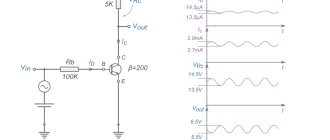
For a common-source field-effect transistor, the family of output characteristics is the dependence of the drain current on the drain-source voltage for various values of the gate-source voltage. The measurement diagram shown in Fig. 6.8, allows you to build appropriate graphs. Required gate-source voltage VGC
set by potentiometer
RV
, and measured by voltmeter
Mx.
Then, using potentiometer
RV2,
a series of drain-source voltage values
VDC
, measured by voltmeter M;
the resulting drain current ID
is measured with a milliammeter
Mu.
A typical family of characteristics of a field-effect transistor is shown in Fig. 6.9.
Rice. 6.8. Measuring circuit for constructing the drain characteristics of a field-effect transistor.
Rice. 6.9. Typical drain characteristics of an i-channel field-effect transistor: A - region of variable resistance; B is the saturation region.
As can be seen from Fig. 6.9, in general terms, the drain characteristics of a field-effect transistor are similar to the collector characteristics of a bipolar transistor: both are a fixed current source over most of the voltage range. In other words, if the gate-source bias is fixed at 1 V, then increasing VDC
5 to 15 V has little effect on drain current. This not at all obvious fact applies to the area of curves to the right of the dotted line; this region is called the saturation region.
To understand the operation of the transistor in this area, you need to consider Fig. 6.10, which schematically shows a field-effect transistor with sources connected to the drain and gate. Initially it can be assumed that VDC
= 0 and the gate voltage
VGC
is such that the depletion layer occupies part of the width of the silicon bar, while the other part of the chip remains a conducting channel between the source and drain.
When VDC
begins to rise from zero, the channel initially behaves simply as a resistor, the resistance of which is determined by the width of the channel left in the chip by the depletion layer.
When VDC reaches several hundred millivolts, reverse bias at the gate begins to take effect and the depletion layer expands, mostly at the positive end of the channel (at the drain), until a very narrow conducting channel remains. Further increases in VDC result in an even narrower channel, almost exactly balancing the expected increase in ID
with increasing voltage.
(This is an error: as V
increases, the length of the channel section with the maximum current density increases, the electric field strength in this section remains unchanged and therefore the drain current does not change. -
Note transl.)
This is the region of maximum compression of the channel (saturation);
in Fig. Figure 6.9 clearly shows the exit from the resistive
region when the curves bend, becoming almost horizontal (the current becomes constant). As with a bipolar transistor, there is a small positive voltage
Rice. 6.10. Ultimate channel compression in a field-effect transistor.
Literature: M.H. Jones, Electronics - practical course Moscow: Tekhnosphere, 2006. - 512 p. ISBN 5-94836-086-5
Tweet Like
- Previous post: The simplest DC amplifier
- Next post: Registers for storing data
- POWER SUPPLY FOR CAR RADIO (0)
- BATTERY CHARGER (0)
- LITHIUM-NON CELL CHARGER CHARGER CONTROLLER (0)
- BATTERY CHARGING CURRENT LIMITER (0)
- SOUND DEVICE FOR MOTORCYCLE SECURITY (0)
- BATTERY VOLTAGE INDICATOR SIMPLE CIRCUIT (0)
- BATTERY VOLTAGE LEVEL INDICATOR (0)
Related posts:
Field effect transistor device
The control electrode of the field effect transistor is called the gate. The channel is formed by a semiconductor of arbitrary conductivity type. Depending on the polarity of the control voltage, it is positive or negative. The field of the corresponding sign displaces free carriers until the isthmus under the gate electrode is completely empty. Achieved by applying a field to either a pn junction or a homogeneous semiconductor. The current becomes zero. This is how a field effect transistor works.
The current flows from source to drain; beginners are traditionally tormented by the question of distinguishing between the two indicated electrodes. There is no difference in which direction the charges move. The field effect transistor is reversible. The unipolarity of charge carriers explains the low noise level. Therefore, field-effect transistors occupy a dominant position in technology.
Transistor design
The key feature of the devices is the large input resistance, especially for alternating current. An obvious fact arising from the control of a reverse-biased pn junction (Schottky junction), or the capacitance of a process capacitor in the area of an insulated gate.
The substrate is often an undoped semiconductor. For field effect transistors with a Schottky gate - gallium arsenide. In its pure form, it is a good insulator, to which the following requirements are imposed as part of the product:
- Absence of negative phenomena at the interface with the channel, source, drain: photosensitivity, parasitic control on the substrate, hysteresis of parameters.
- Thermal stability during technological cycles of product manufacturing: resistance to annealing, epitaxy. No diffusion of impurities into the active layers, resulting in degradation.
- Minimum impurities. The requirement is closely related to the previous one.
- High-quality crystal lattice, minimum defects.
It is difficult to create a layer of significant thickness that meets the list of conditions. Therefore, a fifth requirement is added, which consists in the possibility of gradually growing the substrate to the desired size.
MAIN PARAMETERS OF THE FIELD TRANSISTOR
The saturation current Iс0 in the drain circuit of a transistor connected according to a circuit with a common source, with the gate short-circuited with the source (i.e. at Uз.и=0) is typical only for field-effect transistors with a control pn junction.
The drain current at the operating point can be determined by the following formula [2]:
Ic = Ic0(1-Us.i/Uots)2 (1)
where Uots is the cut-off voltage.
Equation (1) is an approximation for the transmission characteristics of any field-effect transistor (especially with low cutoff voltages).
Cut-off voltage Uots is one of the main parameters characterizing a field-effect transistor. When the gate voltage is numerically equal to the cutoff voltage, the field-effect transistor channel is almost completely blocked, and the drain current tends to zero.
Measuring the true value of the cutoff voltage (with complete blocking of the channel) is quite difficult, since in this case one has to deal with extremely small drain currents, which also depend on the insulation resistance. The reference data for field-effect transistors always indicates at what value of the drain current the cut-off voltage was measured. So, for example, for transistors KP102 voltages Uots were obtained at a drain current of 20 μA, and for transistor KP103 - at a drain current of 10 μA.
The slope of the passage characteristic. The input resistance of field-effect transistors on the control electrode side is 107-109 Ohms for pn junction transistors. Since the input currents of field-effect transistors are extremely small, the current in the output circuit is controlled by the input voltage. Therefore, it is advisable to characterize the amplification properties of a field-effect transistor, as well as electron tubes, by the slope of the transmission characteristic.
Slopeness of field-effect transistors
The maximum value of the slope of the Smax characteristic is achieved at Uz.i=0. In this case, the numerical value of Smax is equal to the conductivity of the field-effect transistor channel at zero bias on its electrodes.
The slope of the characteristic of field-effect transistors is 1-2 orders of magnitude less than that of bipolar transistors, therefore, at low load resistances, the gain of the cascade on a field-effect transistor is less than the gain of a similar cascade on a bipolar transistor.
In most cases, the slope of the characteristic of field-effect transistors is considered a frequency-independent parameter. Therefore, the performance of electronic circuits based on field-effect transistors is limited mainly by the parasitic parameters of the circuit.
We obtain the expression for the slope of the characteristic at the PT operating point using (1):
(2)
where Us.i is the gate-source voltage at which S is calculated;
(3)
Relation (3) allows us to calculate the third using two known parameters.
Breakdown voltage. The breakdown mechanism of a field-effect transistor can be explained by the occurrence of an avalanche process in the gate-channel junction. The gate-channel diode reverse voltage varies along the gate length, reaching a maximum value at the drain end of the channel. This is where the breakdown of the field effect transistor occurs. If the drain and source terminals are swapped, the breakdown voltage will hardly change. For example, in the KP102 transistor, breakdown occurs at a total voltage between the gate and drain equal to 30 V. This voltage is minimal; in fact, the breakdown voltage averages about 55 V, and in some specimens it reaches 120 V [7].
A breakdown does not lead to failure of a PT with a control p-n junction, if the dissipated power does not exceed the permissible value. After a breakdown in normal operating mode, these transistors restore their functionality. This property of pn-junction transistors gives them a certain advantage over MOS transistors, in which a breakdown clearly leads to failure of the device.
However, it is necessary to make a reservation that even for a PT with a p-n junction, breakdown is not always harmless. The degree of its influence on the parameters of the transistor is determined by the value and duration of the current flowing through the gate. Thus, as a result of breakdown, the gate leakage current in normal mode may increase [7].
The dynamic resistance of the channel rк is determined by the expression
This resistance at Us.i = 0 and an arbitrary bias Uz.i can be expressed through the parameters of the transistor [2]:
(4)
At low drain-source voltage near the origin, the FET behaves as a variable ohmic resistance, depending on the gate voltage. This remains true even if the polarity of the drain voltage is changed (see Fig. 4); it is only necessary that the voltage at the gate be greater than that at the drain [5].
Field effect transistors with control pn junction and MeP
In this case, the conductivity type of the gate material is different from that used by the channel. In practice you will see various improvements. The shutter is composed of five areas recessed into the channel. A lower voltage can control the flow of current. Meaning an increase in gain.
Bipolar transistor
The circuits use reverse bias of the pn junction; the stronger, the narrower the channel for current flow. At a certain voltage value the transistor turns off. Forward bias is dangerous to use because the powerful drive circuit can affect the gate contour. If the junction is open, a large current will flow or a high voltage will be applied. Normal mode is ensured by the correct selection of polarity and other characteristics of the power source, and the choice of the operating point of the transistor.
However, in some cases forward gate currents are intentionally used. It is noteworthy that this mode can be used by those MOS transistors where the substrate forms a pn junction with the channel. The moving source charge is divided between the gate and drain. You can find a region where a significant current gain is obtained. The mode is controlled by the shutter. As the current iz increases (up to 100 μA), the circuit parameters deteriorate sharply.
A similar connection is used by the so-called gate frequency detector circuit. The design exploits the rectifying properties of the pn junction between the gate and channel. There is little or no forward bias. The device is still driven by gate current. In the drain circuit, a significant signal amplification is obtained. The rectified voltage for the gate is a blocking voltage and varies according to the input law. Simultaneously with detection, signal amplification is achieved. The drain circuit voltage contains the components:
- Constant component. Not used at all.
- Signal with carrier frequency. It is planted on the ground using filter containers.
- Signal with the frequency of the modulating signal. Processed to extract embedded information.
The disadvantage of a gate frequency detector is considered to be a large coefficient of nonlinear distortion. Moreover, the results are equally bad for weak (quadratic dependence of the operating characteristic) and strong (entering the cutoff mode) signals. Somewhat better are demonstrated by a phase detector based on a two-gate transistor. A reference signal is supplied to one control electrode, and an information component is formed at the drain, amplified by a field-effect transistor.
Despite the large linear distortions, the effect is used. For example, in selective power amplifiers that transmit a narrow spectrum of frequencies in doses. Harmonics are filtered and do not have a big impact on the final quality of the circuit.
Metal-semiconductor (MeS) transistors with a Schottky barrier are almost no different from those with a pn junction. At least when it comes to operating principles. But thanks to the special qualities of the metal-semiconductor transition, products are capable of operating at higher frequencies (tens of GHz, cutoff frequencies in the region of 100 GHz). At the same time, the MeP structure is easier to implement when it comes to production and technological processes. Frequency characteristics are determined by the gate charging time and carrier mobility (for GaAs over 10,000 sq. cm/V s).
Classification and main types of field-effect transistors.
We continue to understand field-effect transistors and in this article we’ll talk about what types of field-effect transistors generally exist and how they differ. And let's start with the fact that the most common type of field-effect transistors are transistors with a MOS structure (metal-oxide-semiconductor). Therefore, field-effect transistors are often simply called MOS transistors (or MOSFETs).
As mentioned in the previous article (here), there are n-channel and p-channel MOSFETs. Their characteristics are almost symmetrical, but there is a slight clarification. In p-channels, unlike n-channels, the carriers are not electrons, but holes, which have lower mobility. It follows from this that the characteristics of p-channel MOSFETs are worse than the corresponding characteristics of n-channel FETs (less saturation current, higher threshold voltage, etc.).
Let's look at where the name metal-oxide-semiconductor (MOS) comes from. Consider the structure of a MOSFET transistor :
As you can see, the gate (metal) is isolated from the channel (semiconductor) by a thin layer of dielectric (oxide). Actually, that’s why such a structure is called MOS