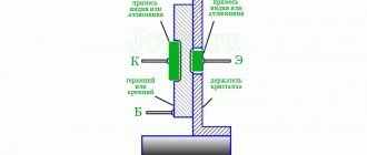
Device
Semiconductor zener diodes have replaced the obsolete glow discharge zener diodes - ion gas-discharge electric vacuum devices. For the manufacture of zener diodes, silicon or germanium crystals (tablets) with n-type conductivity are used, into which impurities are added by an alloy or diffuse alloy method. To obtain an electron-hole pn junction, acceptor impurities, mainly aluminum, are used. The crystals are enclosed in housings made of polymer materials, metal or glass.
Silicon alloy zener diodes D815 (A-I) are produced in a sealed metal case, which is the positive electrode. Such elements have a wide operating temperature range – from -60°C to +100°C. Silicon alloy two-anode stabilizing diodes KS175A, KS182A, KS191A, KS210B, KS213B are produced in a plastic case. Silicon alloy temperature-compensated parts KS211 (B-D), used as reference voltage sources, have a plastic housing.
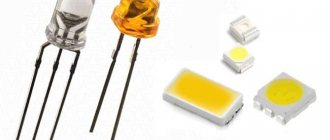
SMD zener diodes, that is, miniature components intended for surface mounting, are manufactured mainly in glass and plastic cases. Such elements can be produced with two or three terminals. In the latter case, the third pin is a “dummy”, does not carry any semantic load and is intended only for reliable fixation of the part on the printed circuit board.
Scheme to check
Let's consider another simple circuit for determining the stabilization voltage, which consists of:
- Regulated power supply. The DC voltage should vary smoothly with a potentiometer from 0 to 50 V (the higher the maximum voltage, the larger the range of elements you can test). This will allow you to test almost any low-power zener diode.
- Set of current limiting resistors. They usually come in denominations of 1 Kom, 2.2 Kom and 4.7 Kom, but there can be more. It all depends on the voltage and current stabilization.
- Voltmeter, you can use an ordinary multimeter.
- Block with spring-loaded contacts. It must have several cells to be able to connect semiconductors with different packages.
To check, connect a zener diode according to the above diagram and gradually increase the voltage at the power source from 0. At the same time, monitor the voltmeter readings. As soon as the voltage on the element stops increasing, regardless of its increase on the power supply, this will be voltage stabilization.
If there is a marking on the element, then the data obtained during measurement is checked against the table in the parameter reference book.
Note that zener diodes can be produced in various designs. For example, KS162 are produced in ceramic cases, KS133 in glass, D814 and D818 in metal.
Here are the characteristics of some common domestic zener diodes:
- KS133a stabilization voltage is 3.3 V, produced in a glass case;
- KS147a maintains voltage at 4.7 V, glass case;
- KS162a – 6.2 V, ceramic body;
- KS175a – 7.5 V, has a ceramic body;
- KS433a – 3.3 V, produced in a metal case;
- KS515a – 15 V, metal housing;
- KS524g – in a ceramic case with a voltage of 24 V;
- KS531v – 31 V, ceramic case;
- KS210b – stabilization voltage 10 V, ceramic body;
- D814a – 7-8.5 V, in a metal case;
- D818b – 9 V, metal case;
- D817b - 68 V, in a metal housing.
To test a zener diode with high stabilization voltages, another circuit is used, which is shown in the figure below.
The check is carried out in the same way as described. Similar devices are produced by Chinese manufacturers.
However, you can assemble a simple circuit for testing zener diodes using a multimeter. This is clearly shown in the video below.
It should be warned that the electrical circuit shown in the video is not recommended for use, because it is unsafe and requires compliance with safety precautions. Otherwise, you may get injured (at best).
Operating principle
The zener diode was discovered by the American physicist Clarence Melvin Zener, after whom it was named. Electrical breakdown of a pn junction can be caused by a tunnel breakdown (in this case, the breakdown is called Zener breakdown), avalanche breakdown, breakdown as a result of thermal instability, which occurs due to destructive self-heating by leakage currents.
And engineers design these elements in such a way that the occurrence of tunneling and/or avalanche breakdown occurs long before they are likely to experience thermal breakdown.
The magnitude of the breakdown voltage depends on the concentration of impurities and the method of doping of the pn junction. The greater the concentration of impurities and the higher their gradient in the junction, the lower the reverse voltage at which a breakdown occurs.
- A tunnel (Zener) breakdown
appears in a semiconductor in cases where the electric field strength in the pn zone is 106 V/cm. Such high voltage can only occur in highly doped diodes. At breakdown voltages in the range of 4.5...6.7 V, the tunnel and avalanche effects coexist, but at a breakdown voltage less than 4.5 V, only the tunnel effect remains. - In zener diodes with low doping levels or smaller gradients of dopant additives there is only an avalanche breakdown mechanism
, which appears at a breakdown voltage of approximately 4.5 V. And at voltages above 7.2 V, only the avalanche effect remains, and the tunnel effect disappears completely.
As mentioned earlier, when connected directly, the zener diode behaves in the same way as a regular diode when connected directly - it passes current. The differences between them arise when connecting in reverse.
A conventional diode, when connected in reverse, blocks the current, and the zener diode, when the reverse voltage reaches a value called the stabilization voltage, begins to pass current in the opposite direction. This is explained by the fact that when a voltage exceeding U nom is applied to the zener diode. device, a process called breakdown occurs in the semiconductor. The breakdown can be tunnel, avalanche, or thermal. As a result of the breakdown, the current flowing through the zener diode increases to a maximum value limited by the resistor. After reaching the breakdown voltage, the current remains approximately constant over a wide range of reverse voltages. The point at which voltage triggers current can be very precisely set during the manufacturing process by doping. Therefore, each element is assigned a certain breakdown (stabilization) voltage.
The zener diode is used only in “reverse bias” mode, that is, its anode is connected to the “-” power supply. The ability of a zener diode to trigger reverse current when the breakdown voltage is reached is used to regulate and stabilize the voltage when the supply voltage or connected load changes. The use of a zener diode makes it possible to provide a constant output voltage for the connected consumer when the power supply voltage drops or the consumer current changes.
What is this element of electrical circuits?
Before we begin to consider the question of what color markings exist for such elements, we need to understand what it is all about.
Volt-ampere characteristic of a zener diode
A zener diode is a semiconductor diode, which is designed to stabilize the DC voltage across the load in an electrical circuit. Most often, such a diode is used to stabilize voltage in various power supplies. This diode (smd) has a section with a reverse branch of the current-voltage characteristic, which is observed in the region of electrical breakdown.
Having such an area, the zener diode in a situation where the parameter of the current flowing through the diode changes from IST.MIN to IST.MAX, practically no changes in the voltage indicator are observed. This effect is used to stabilize voltage. In a situation where the RH load is connected in parallel to the SMD, then the diode voltage will remain constant, and within the specified limits of change in the current flowing through the zener diode.
Note! Zener diode (smd) is capable of stabilizing voltages above 3.3 V.
In addition to SMD, there are also zeners, which are turned on when switched on directly. They are used in situations where there is a need to stabilize the voltage in a certain range. A conventional diode can be used when it is necessary to stabilize the voltage in the range from 0.3 to 0.5 V. The region of their forward bias is observed when the voltage drops to 0.7 - 2v. Moreover, it practically does not depend on the current strength. In their work, stabistors use the direct branch of the current-voltage characteristic. They should also be turned on when connected directly. Although this will not be the best solution, since a zener diode in such a situation will still be more effective. Stabistors, like SMD, are often made from silicon. Zener diodes are labeled according to their main characteristics. This marking looks like this:
- UST. This marking indicates the rated voltage for stabilization;
- ΔUST. Indicates the deviation of the voltage indicator of the rated stabilization voltage;
- IST. Indicates the current that flows through the diode at the rated stabilization voltage;
- IST.MIN - the minimum value of the current that flows through the zener diode. At this value, such an SMD diode will have a voltage in the range UST ± ΔUST;
- IST.MAX. Indicates the maximum permissible amount of current that can flow through the zener diode.
This marking is important when choosing an element for a specific electrical circuit.
Volt-ampere characteristics
The current-voltage characteristic of a zener diode, like a conventional diode, has two branches - forward and reverse. The forward branch is the operating mode for a traditional diode, and the reverse branch characterizes the operation of the zener diode. A zener diode is called a reference diode, and a voltage source that contains a zener diode in its circuit is called a reference diode.
On the working reverse branch of the reference diode, three main values of the reverse current are distinguished:
- Minimum
. When the current is less than the minimum value, the zener diode remains closed. - Optimal
. When the current changes within a wide range between points 1 and 3, the voltage value changes insignificantly. - Maximum
. When applying current above the maximum value, the reference diode will overheat and fail. The maximum current value is limited by the maximum permissible power dissipation, which is highly dependent on external temperature conditions.
The principle of operation of a zener diode
Let's consider the principle of operation of a zener diode using the example of its connection circuit and current-voltage characteristic. To perform its main function, the zener diode VD is connected in series with a resistor Rb and together they are connected to a source of unstabilized input voltage Uin. The already stabilized output voltage Uout is removed only from pins 2, 3 VD. Therefore, the load Rн is connected to the corresponding points 2 and 3. As can be seen from the diagram, VD and Rb form a voltage divider. Only the resistance of the zener diode does not have a constant value and is called dynamic, since it depends on the amount of electric current flowing through the semiconductor device.
The voltage Uin supplied to the zener diode from the resistors must be at least a couple of volts higher than the output voltage Uout, otherwise the semiconductor device VD will not open and will not be able to perform its main function.
Let's say that at some arbitrary point in time at outputs 1 and 3 the value of Uin began to increase. The following processes will begin to occur in the circuit. As the voltage increases, according to Ohm's law, the current will begin to increase, let's call it the input current Iin. As the current increases, the voltage drop across the resistor Rb will increase, and at VD it will remain unchanged (this will be explained further in the characteristic), therefore Uout will remain at the same level. Consequently, the increase in input voltage will drop or be extinguished by resistor Rb. Therefore, Rb is called damping or ballast.
Areas of use
The main area of application of these elements is stabilization of direct voltage in low-power power supplies or in individual units with a power of no more than tens of watts. With the help of reference diodes, they ensure the normal operating mode of transistors, microcircuits, and microcontrollers.
In simple design stabilizers, the zener diode is both a reference voltage source and a regulator. In more complex designs, the zener diode serves only as a source of reference voltage, and an external power transistor is used for power regulation.
Temperature-compensated zener diodes and parts with a hidden structure are in demand as discrete and integrated reference voltage sources. To protect electrical equipment from overvoltages, pulse avalanche zener diodes have been developed. To protect the inputs of electrical devices and the gates of field-effect transistors, ordinary low-power zener diodes are installed in the circuit. Insulated gate field-effect transistors (IGFETs) are manufactured with a single chip on which are located: a protective zener diode and a power transistor.
Main characteristics
The passport of the stabilizing diode indicates the following parameters:
- Rated stabilization voltage Ust
. This setting is selected by the device manufacturer. - Operating current range
. Minimum current – the current value at which the stabilization process begins. Maximum current is the value above which the device is destroyed. - Maximum power dissipation
. In low-power elements this is the nameplate value. In the passports of high-power zener diodes, to calculate the cooling conditions, the manufacturer indicates: the maximum permissible temperature of the semiconductor and the coefficient of thermal resistance of the housing.
In addition to the parameters indicated in the passport, zener diodes are characterized by other quantities, including:
- Differential resistance
. This property determines the instability of the device in terms of supply voltage and load current. The first drawback is eliminated by powering the stabilizing diode from a direct current source, and the second by connecting a DC buffer amplifier with an emitter follower between the zener diode and the load. - Temperature coefficient of voltage
. In accordance with the standard, this value is equal to the ratio of the relative change in stabilization voltage to the absolute change in outside temperature. In non-heat-stabilized zener diodes, when heated from +25°C to +125°C, the stabilization voltage shifts by 5-10% from the original value. - Drift and noise
. These characteristics are not defined for conventional zener diodes. For precision devices they are very important properties. In conventional (non-precision) zener diodes, noise is created by: a large number of foreign impurities and crystal lattice defects in the region of the pn junction. Methods for reducing noise (if necessary): protective passivation with oxide or glass (impurities are directed deep into the crystal) or by moving the pn junction itself deep into the crystal. The second method is more radical. It is in demand in low noise diodes with a hidden structure.
Main types and sizes of SMD devices
Housings of components for microelectronics that have the same nominal values may differ from each other in dimensions. Their dimensions are determined primarily by the standard size of each. For example: resistors are designated by standard sizes from “0201” to “2512”. These 4 digits in the SMD component marking indicate a coding that indicates the length and width of the device in inch measurements. In the table provided, typical dimensions are also indicated in mm.
Marking of SMD components - resistors
| Square Chip Resistors and Ceramic Capacitors | |||||
| Standard size | L, mm (inch) | W, mm (inch) | H, mm (inch) | A, mm | W |
| 0201 | 0.6 (0.02) | 0.3 (0.01) | 0.23 (0.01) | 0.13 | 1/20 |
| 0402 | 1.0 (0.04) | 0.5 (0.01) | 0.35 (0.014) | 0.25 | 1/16 |
| 0603 | 1.6 (0.06) | 0.8 (0.03) | 0.45 (0.018) | 0.3 | 1/10 |
| 0805 | 2.0 (0.08) | 1.2 (0.05) | 0.4 (0.018) | 0.4 | 1/8 |
| 1206 | 3.2 (0.12) | 1.6 (0.06) | 0.5 (0.022) | 0.5 | 1/4 |
| 1210 | 5.0 (0.12) | 2.5 (0.10) | 0.55 (0.022) | 0.5 | 1/2 |
| 1218 | 5.0 (0.12) | 2.5 (0.18) | 0.55 (0.022) | 0.5 | 1 |
| 2010 | 5.0 (0.20) | 2.5 (0.10) | 0.55 (0.024) | 0.5 | 3/4 |
| 2512 | 6.35 (0.25) | 3.2 (0.12) | 0.55 (0.024) | 0.5 | 1 |
| Cylindrical chip resistors and diodes | |||||
| Standard size | Ø, mm (inch) | L, mm (inch) | W | ||
| 0102 | 1.1 (0.01) | 2.2 (0.02) | 1/4 | ||
| 0204 | 1.4 (0.02) | 3.6 (0.04) | 1/2 | ||
| 0207 | 2.2 (0.02) | 5.8 (0.07) | 1 |
SMD capacitors
Capacitors made of ceramic are the same size as resistors; as for tantalum capacitors, they are determined according to their own standard size scale:
| Tantalum capacitors | |||||
| Standard size | L, mm (inch) | W, mm (inch) | T, mm (inch) | B, mm | A, mm |
| A | 3.2 (0.126) | 1.6 (0.063) | 1.6 (0.063) | 1.2 | 0.8 |
| B | 3.5 (0.138) | 2.8 (0.110) | 1.9 (0.075) | 2.2 | 0.8 |
| C | 6.0 (0.236) | 3.2 (0.126) | 2.5 (0.098) | 2.2 | 1.3 |
| D | 7.3 (0.287) | 4.3 (0.170) | 2.8 (0.110) | 2.4 | 1.3 |
| E | 7.3 (0.287) | 4.3 (0.170) | 4.0 (0.158) | 2.4 | 1.2 |
SMD Inductors and Chokes
Inductive coils can be made in various housing configurations, but their value is also indicated based on the standard sizes. This principle of SMD marking and decoding of codes makes it possible to significantly simplify the installation of elements on the board in automatic mode, and for the radio amateur to navigate more freely.
dr>
Winding components such as coils, transformers and others, which in most cases we make ourselves, may simply not fit on the board. Therefore, such products are also available in compact versions that can be installed on a board.
To determine which coil your project requires, it is best to use the catalog and select the required option according to the standard size there. Typical sizes are determined using a code marking marked with 4 numbers (0805). Where "08" is the length and "05" is the width in inches. The actual dimensions of such an SMD component will be 0.08x0.05 inches.
Diodes and Zener diodes in SMD housing
As for diodes, they are also available in both cylindrical and polyhedron-shaped cases. The typical dimensions of these components are set identically to inductive coils, resistors and capacitors.
| Diodes, Zener diodes, capacitors, resistors | |||||
| Type of shell | L* (mm) | D* (mm) | F* (mm) | S* (mm) | Note |
| DO-213AA (SOD80) | 3.5 | 1.65 | 048 | 0.03 | JEDEC |
| DO-213AB (MELF) | 5.0 | 2.52 | 0.48 | 0.03 | JEDEC |
| DO-213AC | 3.45 | 1.4 | 0.42 | — | JEDEC |
| ERD03LL | 1.6 | 1.0 | 0.2 | 0.05 | PANASONIC |
| ER021L | 2.0 | 1.25 | 0.3 | 0.07 | PANASONIC |
| ERSM | 5.9 | 2.2 | 0.6 | 0.15 | PANASONIC, GOST R1-11 |
| MELF | 5.0 | 2.5 | 0.5 | 0.1 | CENTS |
| SOD80 (miniMELF) | 3.5 | 1.6 | 0.3 | 0.075 | PHILIPS |
| SOD80C | 3.6 | 1.52 | 0.3 | 0.075 | PHILIPS |
| SOD87 | 3.5 | 2.05 | 0.3 | 0.075 | PHILIPS |
Transistors in SMD housing
SMD transistors are made in packages that correspond to their maximum power. The cases of these semiconductor elements can be symbolically divided into two types: SOT and DPAK.
Marking of SMD components
Labeling electronic devices in modern technology already requires professional knowledge, and it’s so simple that it’s hard to understand at first glance, especially for a novice radio amateur. In comparison with parts produced in the Soviet Union, where the marking of the nominal value and type of device was applied in text form, now this is simply a soldering tool meta. There was no need to keep piles of reference literature on hand to determine the purpose and parameters of a particular device.
However, technological processes in industry do not stand still and production automation determines its own rules. It is SMD parts that play the main role in surface mounting, and the robot does not care about marking the parts inserted into the machine; what is placed there, it solders. The marking is needed by the specialist who services this robot.
Download a program to decipher the designation of SMD parts
Connection methods - serial and parallel
For imported parts in the accompanying documents, situations in which a serial or parallel connection is possible are not regulated. In the documentation for domestic reference diodes you can find two instructions:
- In devices of small and medium power, any number of single-series zener diodes can be connected in series or in parallel.
- In devices of medium and high power, any number of stabilizing diodes of a single series can be connected in series. For a parallel connection, calculations must be made. The total power dissipation of all parallel-connected zener diodes should not be higher than that of one part.
It is possible to connect reference diodes of different series in series if the operating currents of the created circuit do not exceed the rated stabilization currents for each series installed in the circuit.
In practice, to multiply the stabilization voltage, a series connection of two or three zener diodes is most often used. This measure is resorted to if it was not possible to obtain a part for the required voltage or it is necessary to create a high-voltage zener diode. When connected in series, the voltage of the individual elements is summed. This type of connection is mainly used in the assembly of high-voltage stabilizers.
Parallel connection of parts serves to increase current and power. However, in practice, this type of connection is rarely used, since different instances of reference diodes, even of the same type, do not have exactly the same stabilization voltages. Therefore, with a parallel connection, a discharge will occur only in the part with the lowest stabilization voltage, and breakdown will not occur in the rest. If a breakdown occurs, then some zener diodes in such a circuit will operate with underload, and others with overload.
To stabilize the alternating voltage, the zener diodes are connected in series and back-to-back. In the first half-cycle of an alternating current sinusoid, one element operates as a regular diode, and the second performs the functions of a zener diode. In the second half-cycle, the elements change functions. The output voltage shape is different from the input voltage. Its configuration resembles a trapezoid. This is due to the fact that a voltage exceeding the stabilization voltage will be cut off and the tops of the sine wave will be cut off. Series and counter connection of zener diodes can be used in a temperature-stabilized zener diode.
What it is
The literature gives the following definition:
A Zener diode or Zener diode is a device designed to stabilize voltage in electrical circuits. Operates under reverse bias in breakdown mode. Before breakdown occurs, it has a high transition resistance. The currents flowing in this case are insignificant. Widely used in electronics and electrical engineering.
In simple terms, a zener diode is designed to stabilize voltage in electronic circuits. It is connected to the circuit in the opposite direction. When a voltage exceeds the stabilization voltage, a reversible electrical breakdown of the pn junction occurs. As soon as it drops to nominal, the breakdown stops and the zener diode closes.
The figure below is a graphical diagram for dummies to help you understand the working principle of a Zener diode.
The main advantages are low cost and small dimensions. The industry produces devices with stabilization voltages of 1.8 - 400 V in metal, ceramic or glass cases. This depends on the power for which the zener diode is designed and other characteristics.
To stabilize high-voltage voltages from 0.4 to several tens of kV, glow discharge zener diodes are used. They have a glass body and, before the advent of semiconductor devices, were used in parametric stabilizers.
Devices that change their resistance depending on the applied voltage have similar properties - these are varistors. The difference between a zener diode and a varistor is that the latter has bidirectional symmetrical characteristics. This means that, unlike diodes, it has no polarity. Briefly, a varistor is designed to provide overvoltage protection to electronic circuits.
Suppressors are used to protect equipment from power surges. The differences between a zener diode and a suppressor are that the former gradually changes its internal resistance depending on the applied voltage. The second one opens immediately when a certain voltage threshold is reached. Those. its internal resistance tends to zero. The main purpose of suppressors is to protect equipment from power surges.
The figure below shows the conventional graphic designation (UGO according to GOST) of a semiconductor and its current-voltage characteristic.
The numbers in the figure indicate area 1-2. It is working and is designed to stabilize voltage in circuits. If the device is turned on in the forward direction, it will work like a regular diode.
We recommend watching the following video to learn more about the principle of operation of a zener diode, the designation of elements and their scope of application.
Composite Zener diodes
Composite zener diode is a device used in situations where currents and power greater than those allowed by technical conditions are required. In this case, a DC buffer amplifier is connected between the stabilizing diode and the load. In the circuit, the collector junction of the transistor is connected in parallel with the stabilizing diode, and the emitter junction is connected in series.
The circuit of a conventional composite zener diode is not intended for direct current use. But adding a diode bridge turns the compound zener diode into a dual-acting system that can operate with both forward and reverse current. Such zener diodes are also called double or two-anode. Zener diodes that can operate with voltage of only one polarity are called asymmetrical. And composite zener diodes, capable of operating in any direction of current, are called symmetrical.
Types of Zener diodes
On the modern electronics market there is a wide range of zener diodes adapted to specific application conditions.
Precision
These devices provide high output voltage stability. They are subject to additional requirements regarding the temporary instability of voltage and temperature coefficient of voltage. Precision devices include:
- Temperature compensated
. The temperature-compensated zener diode circuit includes a series-connected zener diode with a nominal voltage of 5.6 V (with a positive temperature coefficient) and a directly illuminated diode (with a negative coefficient). When these elements are connected in series, mutual compensation of temperature coefficients occurs. Instead of a diode, a second zener diode can be used in the circuit, connected in series and counter. - With hidden structure
. The breakdown current in a conventional zener diode is concentrated in the near-surface silicon layer, where the maximum amount of foreign impurities and crystal lattice defects is located. These design imperfections cause noise and unstable operation. In parts with a hidden structure, the breakdown current is “driven” inside the crystal by forming a deep island of p-type conductivity.
Fast acting
They are characterized by: a low value of the barrier capacitance, only tens of picofarads, and a short period of the transient process (nanoseconds). Such features allow the reference diode to limit and stabilize short-term voltage pulses.
Stabilizing diodes can be designed for stabilization voltages from several volts to several hundred volts. High-voltage zener diodes are installed on special coolers that can provide the necessary heat exchange and protect the element from overheating and subsequent destruction.
Adjustable Zener Diodes
When manufacturing stabilized power supplies, the necessary zener diode may be missing. In this case, an adjustable zener diode circuit is assembled.
The required voltage of the stabilizing diode is selected using resistor R1. To configure the circuit, a variable resistor with a nominal value of 10 kOhm is connected in place of resistor R1. After obtaining the required voltage value, determine the resulting resistance and install a resistor of the required value in a permanent place. For this circuit, you can use transistors KT342A, KT3102A.
Marking methods
On the body of the part there is an alphabetic or alphanumeric marking that characterizes the electrical properties and purpose of the device. There are two types of markings. Parts in a glass case are marked in the usual way. The stabilization voltage is written on the surface of the element using the letter V, which acts as a decimal point. The marking of four numbers and a letter at the end is less clear. It can only be decrypted using a datasheet.
Another way to designate stabilizing diodes is by color coding. The Japanese version is often used, which consists of two or three colored rings. If there are two rings, each of them represents a specific number. If the second ring is applied in double form, this means that a comma must be placed between the first and second digits.
Details about the color coding of the stabilizing diode
Any diode (zener diode, etc.) contains a special marking on its case, which reflects what material was used to manufacture each specific semiconductor. Such marking may look like this:
In addition, the marking reflects the electrical properties and purpose of the device. Usually a number is responsible for this. The letter, in turn, reflects the corresponding type of device. In addition, the marking contains the date of manufacture and the symbol of the product. Integral type SMDs often contain full markings. In such a situation, there is a conditional code on the product body that indicates the type of microcircuit. An example of decoding the code markings for microcircuits applied to the housing is shown in the figure:
Example of microcircuit marking
In addition, there is also color coding. It exists in several versions, but the most commonly used is the Japanese marking (JIS-C-7012). The color coding is shown in the following table.
How to distinguish a zener diode from a regular diode
Both of these elements have a similar designation in the diagram. In practice, you can distinguish a zener diode from a regular diode and even find out its rating, if it is no more than 35 V, using a multimeter attachment.
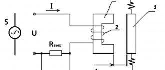
Multimeter attachment circuit
To implement a pulse-width modulation generator, a specialized MC34063 microcircuit is used. To ensure galvanic isolation between the power supply and the measuring part of the circuit, the voltage is controlled on the primary winding of the transformer. This allows you to make a rectifier on VD2. The output voltage stabilization point is set using resistor R3. The voltage on capacitor C4 is approximately 40 V. Current stabilizer A2 and the reference diode being tested constitute a parametric stabilizer, and a multimeter connected to the terminals of the circuit allows you to determine the voltage of the zener diode.
If the diode is connected in reverse polarity (anode to “-” and cathode to “+”), then the multimeter for a conventional diode will show 40 V, and for a zener diode - stabilization voltage.
To determine the performance of a zener diode with a known rating, a simple circuit is used, consisting of a power source and a current-limiting resistor of 300...500 Ohms. In this case, a multimeter is used to determine not the junction resistance, but the voltage. Switch on the elements as shown in the diagram and measure the voltage on the zener diode.
Slowly increase the voltage of the power supply. At the value of the stabilization voltage, the voltage on the zener diode should stop growing. If this happens, it means the element is working. If, with a subsequent increase in the IP voltage, the diode does not begin to stabilize, it means that it is not working properly.
Operating principle of stabilization diodes
Despite the fact that the SMD is similar to a diode, it is essentially a different element of the electrical circuit. Of course, it can serve as a rectifier, but is usually used to stabilize the voltage. This element is capable of maintaining a constant voltage in a DC circuit. This principle of operation is used in power supply of various radio equipment.
Zener diode and diode
Externally, SMD is very similar to a standard semiconductor. The similarity remains in the design features. But when designating such a radio element, unlike a diode, the letter G is placed on the diagram. If you do not delve into mathematical calculations and physical phenomena, then the operating principle of smd will be quite clear.
Note! When turning on such an SMD diode, you must observe reverse polarity. This means that the connection is made with the anode to the minus.
Passing through this element, a small voltage in the circuit provokes a strong current. As the reverse voltage increases, the current also increases, only in this case its growth will be observed weakly. When you reach the mark, it can be anything. It all depends on the type of device. When the mark is reached, a “breakdown” occurs. After the “breakdown” has occurred, a large reverse current begins to flow through the smd. It is at this moment that the operation of this element begins until its permissible limit is exceeded.
How to choose the right zener diode?
Zener diodes are low power stabilizers. Therefore, they must be selected so that the entire load current plus the minimum stabilization current can pass through them without overheating.
To correctly select a zener diode for an electrical circuit, you need to know the following parameters: minimum and maximum input voltage, output voltage, minimum and maximum load current. The stabilization voltage of the zener diode is equal to the output voltage. And it is best to calculate the maximum current that can pass through a zener diode in a particular circuit, and the power dissipation at the maximum current, using an online calculator.
Diode in AC circuit
For those who have forgotten what alternating current is, read. So, in order to consider the operation of a diode in an alternating current circuit, let's draw a diagram. Here we see a frequency generator G, a diode and two terminal blocks X1 and X2, from which we will take a signal using an oscilloscope.
My frequency generator looks like this.
frequency generator
We will take an oscillogram using a digital oscilloscope
The generator produces alternating sinusoidal voltage.
sine wave
What happens after the diode? We connect to terminals X1 and X2 and see this oscillogram.
AC voltage after diode
The diode cut out the bottom part of the sine wave, leaving only the top part.
What happens if we change the diode leads? The scheme will look like this.
alternating current after diode
What do we get at terminals X1 and X2? Let's look at the oscillogram.
alternating current after diode
Wow! The diode cut off only the positive part of the sine wave!