Microelectronics is a fashionable hobby in recent years thanks to the magical Arduino. But here’s the problem: with enough interest, you can quickly outgrow DigitalWrite(), but what to do next is not entirely clear. Arduino developers have put a lot of effort into lowering the barrier to entry into their ecosystem, but outside it there is still a dark forest of harsh circuitry that is inaccessible to the amateur.
For example, datasheets. It seems like they have everything, take it and use it. But their authors clearly do not set themselves the task of popularizing microcontrollers; sometimes it seems that they deliberately abuse obscure terms and abbreviations when describing simple things in order to confuse the uninitiated as much as possible. But not everything is so bad; if desired, the casket opens.
In this article I will share the experience of a humanities specialist communicating with datasheets for hobby purposes. The text is intended for amateurs who have grown up from Arduino pants; it assumes some understanding of the principles of operation of microcontrollers.
I'll start with the traditional
Flashing an LED on Arduino
And immediately the code:
void setup() { DDRB |= (1<<5); } void loop() { PINB = (1<<5); for (volatile uint32_t k=0; k<100000; k++); }
"What is this? – A sophisticated reader will ask. – Why are you writing something to the PINB input register? It’s for reading only!” Indeed, the Arduino documentation, like most educational articles on the Internet, states that this register is read-only. I thought so myself until I re-read the datasheet for the Atmega328p while preparing this article. And there:
This is a relatively new functionality, it was not on Atmega8, not everyone knows about it or is not mentioned for reasons of backward compatibility. But it is quite suitable for demonstrating the idea that datasheets are worth reading in order to use all the capabilities of the chip, including little-known ones. And this is not the only reason.
Why else read datasheets?
Usually, Arduino engineers, having played enough with LEDs and AnalogWrites, begin to connect all sorts of modules and chips to the board, for which there are already written libraries. Sooner or later, a library appears that does not work as it should. Then the amateur starts picking at it to fix it, and then...
And something completely incomprehensible happens there, so you have to go to Google, read numerous tutorials, pull out parts of someone’s suitable code and finally achieve your goal. This gives a powerful sense of accomplishment, but in reality the process is like reinventing the wheel by reverse engineering a motorcycle. Moreover, the understanding of how this bike works does not increase. I know, because I did this myself for quite a long time.
If instead of this exciting activity I had spent a couple of days studying the Atmega328 documentation, I would have saved a huge amount of time. After all, this is a fairly simple microcontroller.
Thus, you need to read datasheets at least in order to imagine how the microcontroller generally works and what it can do. And further:
- to check and optimize other people's libraries. They are often written by the same amateurs who reinvent the wheel; or, on the contrary, the authors deliberately make them excessively foolproof. Let it be three times larger and slower, but it will definitely work;
- to be able to use chips in a project for which no one has written a library;
- to make it easier for yourself to migrate from one MK line to another;
- to finally optimize your old code, which did not fit into Arduino;
- to learn how to control any chip directly through its registers, without bothering with studying the structure of its libraries, if any.
Universal programmer CH341A - application in work
The connection of flash memory chips of the 25xx series with SOP8/SOP16 housing design to the programmer is carried out through the corresponding contact pads. Two such pads are located directly on the circuit board of the CH341A programmer next to the ZIF panel.
Universal programmer CH431A and a set of additional elements. A miniature board with holes for pins, on the reverse side there are pads for SOP chips. An additional circuit board is also supplied with the CH341A programmer. This accessory is used for programming memory chips with SOP8/SOP16 architectural designs. For in-circuit programming, the circuit board of the CH341A programmer contains a 3.3-volt power contact and the corresponding ISP interface contacts:
- MOSI;
- MISO;
- CLK;
- CS;
- GND.
At the same time, it is possible to work with peripherals via the RS232 interface (pins on the board RX, TX, GND). The CH341A programmer circuit is designed for power supply with a constant voltage of 5 volts from an external source. This voltage, when the programmer is connected to a personal computer, is supplied via the USB bus.
CH341A programmer for memory chips connected to the computer's USB port. The glow of the red indicator indicates the presence of power in the device circuit. The programmer's printed circuit board has a built-in power supply indicator - a red LED. The external or internal programming mode is activated by removing or installing a jumper on the P/S (parallel/serial) contacts, also integrated into the CH341A programmer circuit. By default the jumper is set.
The position of the installed jumper on the P/S (parallel/serial) contacts of the CH341A programmer corresponds to the internal programming mode. In this case:
- reading,
- verification,
- recording memory chips,
carried out directly through the ZIF panel of the CH341A programmer. Meanwhile, on the CH341A universal programmer board, the jumper can be removed from the P/S (parallel/serial) pins. Programming in this mode allows direct connection to the programmable memory chip without desoldering it from the board.
CH341A Programmer - Firmware/Read Software
The operation of the CH341A universal physical module at the software level is supported by the “parent” software - “CH341A Programmer” (here version 1.4).
Drivers used for operating systems and interfaces:
- under Windows 10 and earlier on IIC / I2C, SPI and others;
- under Windows 10 and earlier on a serial interface;
- for Linux;
- for Mac;
distributed free of charge on the Internet.
The interface of the working program window of software version 1.30 is easy to perceive and understand for both novice electronics engineers and professionals. All main designations of the software interface of version 1.30 have been translated into Russian. In general, the program supports several regional interface languages. However, version 1.4 (English interface) is also presented above.
This is what the software window for the CH341A programmer looks like. A convenient, easy-to-read and understand interface that supports notations in Russian. Of course, in order for the software to be successfully connected to the device and to be programmed correctly and efficiently, installation of system drivers is required. These are components that complement the software and are usually included in the software installation package.
When you connect the programmer to a USB port, the system automatically displays (older versions of Windows only) a message about the need to install device drivers. You just need to specify the path to the folder where the required files are located. Latest versions (eg Windows 10) require digitally signed files. Here above you can download official digitally signed drivers.
Subtleties of programming memory chips via the CH341A interface
A logical question for novice electronics engineers: how to flash an eeprom memory chip in a DIP package using this device? So, working with EEPROM memory chips (24xx, 25xx) in a DIP package is carried out approximately as follows (subject to pre-installed drivers):
- On the ZIF panel, install the handle perpendicular to the body.
- Insert the microcircuit into the cell according to the designation on the board 24xx or 25xx (1 leg closer to the handle).
- Lower the handle to a position parallel to the panel body.
- Connect the CH341A programmer to the USB port.
- Connect the device in Windows Manager.
- Launch Programmer and perform the required actions (reading, flashing, comparing checksums, etc.).
The video above shows the sequence of working with memory chips through the software support environment. In particular, examples of working with the “Programmer CH341A” software of two versions (1.30 and 1.4, respectively) are shown. After completing work with the software, it is recommended to disable the device in the Windows Manager list (not delete, but deactivate).
Programming chips from the 25xx flash memory series with SOP packages is done a little differently. The ZIF contact panel can also be used in this case, but provided that the microcircuit is mounted on an additional printed circuit board.
An additional printed circuit board must be equipped with contact electrodes by soldering the electrodes into the corresponding holes on the board. The operational (programmable) microcircuit will also have to be soldered onto the contact pads.
Meanwhile, there is a simplified way of communication. The main board of the CH341A programmer has pads for SOP configuration. A programmable chip is carefully placed on such a pad so that the legs of the microcircuit exactly fall on the contact tracks.
Contact pads for placement of memory chips in SOP type housing. Two pads for the 25xx series and one for the 24xx series. You should check that the location of the chip matches the key on the case and on the board. There is a contact indicator for the first leg of the chip. The chip is then gently pressed with a miniature clothespin. Then everything is done in the standard way - connecting to a computer port and programming the chip.
Programmer CH341A: where to buy and what is the price
It is more profitable to buy a device on the well-known Aliexpress portal. The price stated by Chinese sellers is purely symbolic (no more than 200 rubles including shipping). A faster and easier purchase is made through the federal Yandex Market. Suggestions below:
The only inconvenience for the buyer in case of a request through the Chinese shop-portal AliExpress is that he has to wait about a month or a month and a half for the parcel to arrive in Russia. But if you take into account the opportunities that open up with the purchase of this product, you can wait 3 months.
The page of one of the Aliexpress sellers offering the CH341A programmer to buy for 112 rubles. This offer has been verified - you can safely buy, for example, for Yandex money. Memory chips from the following manufacturers are available to read and “flash” with the CH341A programmer:
- Atmel;
- Amic;
- EON;
- ST;
- Excel Semiconductor Inc;
- NexFlash;
- MXIC;
- Chingis Technology Corporation;
- WINBOND;
- Saifun Semiconductors.
Table of supported chips by CH341A programmer
| ATMEL | AT25DF041A, AT25DF321, AT25F004, AT25F512A, AT25F2048, AT25F4096, AT25F1024A, AT25FS010, AT25FS040, AT26DF081A,AT26DF161A, AT26DF321, AT26F004 |
| AMIC | A25L05P, A25L10P, A25L20P, A25L40P, A25L80P, A25L16P |
| EON | EN25B05, EN25P05, EN25B10, EN25P10, EN25BF20, EN25P20, EN25F20, EN25B40, EN25P40, EN25F40, EN25B80, EN25P80, EN25F80, EN25T80, EN25B16, EN2 5P16, EN25B32, EN25P32, EN25B64, EN25P64 |
| ST | M25P05A, M25P10A, M25P20, M25P40, M25P80, M25P16, M25P32, M25P64, M25PE10, M25PE20, M25PE40, M25PE80, M25PE16, M25PE32, M45PE10, M45PE20, M45PE40, M45 PE80, M45PE16, M45PE32 |
| EXCEL SEMICONDUCTOR INC | ES25P10, ES25P20, ES25P40, ES25P80, ES25P16, ES25P32 |
| NEXFLASH | NX25P80, NX25P16, NX25P32 |
| MXIC | MX25L512, MX25L1005, MX25L2005, MX25L4005, MX25L8005, MX25L1605, MX25L3205, MX25L6405, MX25L6445, MX25L6405 |
| CHINGIS TECHNOLOGY CORPORATION | Pm25LV512, Pm25LV010, Pm25LV020, Pm25LV040, Pm25LV080, Pm25LV016, Pm25LV032, Pm25LV064 |
| WINBOND | W25P10, W25X10, W25Q10, W25P20, W25X20, W25Q20, W25P40, W25X40, W25Q40, W25P80, W25X80, W25Q80, W25P16, W25X16, W25Q16, W25P32, W25X32, W25Q3 2, W25P64, W25X64, W25Q64 |
| SAIFUN | SA25F005, SA25F010, SA25F020, SA25F040, SA25F080, SA25F160, SA25F320 |
The table above represents a far from complete list of companies whose memory chips are available for reading and writing code with the CH341A programmer.
After reading the contents of the chip by the device, the program saves the files to the specified folder with the extension *.bin (binary). This point in the programming process must be taken into account.
For example, when dump files obtained from other sources with other types of extensions are used for new firmware of a microcircuit. Before loading by the programmer, such files need to be replaced with the default extension (*.bin).
How to flash a memory chip without desoldering
The memory chip programmer was tested by reading the eeprom memory dump of the Pixel controller (2 pcs. ATMLH132). The work of reading information, which could not be done using other programmer designs, required no more than 3-4 seconds of time. At the same time, readable memory chips were not soldered off from the controller board.
The Pixel controller memory module, consisting of two 24 series memory chips, was directly connected to the CH341A programmer interface. The connection was made via a standard 4-pin connector. Experience - how to read a dump from a 24C04 series microcircuit without soldering the chip from the board is described below.
Reading a dump of memory chips using the CH341A programmer
To be able to connect to microcircuits in DIP packages directly on the board, you need to acquire a contact “clothespin”. This tool can also be purchased inexpensively from the website mentioned earlier.
A set of accessories for the programmer, which includes a contactor clip for microcircuits in a DIP case and an adapter board that makes contact with the ZIF panel. The clothespin is installed on the chip body in such a way that all contacts fit exactly on the legs of the programmable chip. The first contact leg of the working microcircuit must correspond to the contact of the “clothespin” with the connected red wire.
The board with the working chip on which the dump is written or removed must be disconnected from any power sources,
including lithium-ion batteries (relevant for computer motherboards). On the CH341A programmer, the jumper on the “P/S” contacts is removed.
An example of connecting a cable with a clothespin to a programmable memory chip. The conductor marked in red corresponds to the contact with the first leg of the chip. The mating end of the cable with a “clothespin” is connected to an adapter (mini-board) via a pin connection, and then to the ZIF panel of the CH341A programmer. Depending on the type of programmable microcircuit, the adapter board is installed in the contact sockets for chips of the 24xx or 25xx series.
Then all that remains is to plug in the CH341A programmer into the USB port, launch the accompanying program on the computer, and you can start working with the memory chip dump. For example, for the specified series of 24C04 microcircuits, it took no more than 3 seconds to read the dump:
The result of working with a memory chip in full contact with the device board. The dump was taken without unsoldering the chip from the device board. Some memory chips designed for a supply voltage of 5 volts sometimes do not respond to the actions of the CH341A programmer. This is expressed as a result when the dump is not read or written.
The reason for the lack of read/write on the CH341A programmer
The reason for the lack of operating effect is explained simply: by default, the CH341A programmer circuit uses an operating voltage (stabilized from USB) equal to 3.3 volts. With such a low voltage level and a current not exceeding 500 mA, some series of chips simply “do not enter” the programming mode.
Schematic diagram of the CH341A programmer, designed for programming memory chips of the 24xx (eeprom) and 25xx (flash memory) series. In addition, current losses through the capacitances of the electronic board where the operating chip is installed should be taken into account. For such cases, a sufficient operating level of programming voltage is required, as well as a sufficiently high current potential.
Accordingly, eliminating the cause is to supply programming voltage directly from a more powerful external power source. To do this, use the 7-pin connector present on the CH341A programmer board. The designation of the connector contacts is on the circuit diagram (see above).
Why write to registers directly when there is HAL and LL?
Dictionary HAL, Hardware Abstraction Layer - a library for controlling a microcontroller with a high level of abstraction. If you need to use the SPI1 interface, you simply configure and enable SPI1 without thinking about which registers are responsible for what. LL, Low Level API - a library containing macros or structures with register addresses, allowing you to access them by name. DDRx, PORTx, PINx on Atmega are LL.
Disputes on the topic “HAL, LL or registers” regularly occur in comments on Habré. Without claiming access to astral knowledge, I will simply share my amateur experience and thoughts.
Having more or less figured out Atmega and having read articles about the wonderfulness of STM32, I bought half a dozen different boards - Discovery, and Blue Pills, and even just chips for my homemade products. They all collected dust in a box for two years. Sometimes I said to myself: “that’s it, starting this weekend I’m mastering STM,” launched CubeMX, generated a setup for SPI, looked at the resulting wall of text, generously flavored with STM copyrights, and decided that this was somehow too much.
Of course, you can figure out what CubeMX wrote here. But at the same time it is clear that remembering all the wording and then writing them by hand is unrealistic. And to debug this, if I accidentally forget to check a box in the Cube, that’s totally fine.
Two years passed, I was still licking my lips in the ST MCU Finder at all sorts of tasty, but beyond my understanding, chips, and accidentally came across a wonderful article, albeit about STM8. And suddenly I realized that all this time I had been knocking on an open door: the registers of the STM are arranged in the same way as those of any other MK, and the Cube is not necessary to work with them. Was it even possible?..
HAL and specifically STM32CubeMX is a tool for professional engineers who work closely with STM32 chips. The main feature is a high level of abstraction, the ability to quickly migrate from one MCU to another and even from one core to another, while remaining within the STM32 line. Hobbyists rarely encounter such problems - our choice of microcontrollers, as a rule, is limited to the AliExpress assortment, and we often migrate between radically different chips - we move from Atmega to STM, from STM to ESP, or whatever new thing our Chinese friends throw at us. HAL will not help here, and studying it will eat up a lot of time.
LL remains - but from it to the registers there is half a step. Personally, I find writing my macros with register addresses useful: I study the datasheet more carefully, I think about what I will need in the future and what I definitely won’t, I structure my programs better, and in general, overcoming helps memorize.
In addition, there is a nuance with the popular STM32F103 - there are two incompatible LL versions for it, one official from STM, the second from Leaf Labs, used in the STM32duino project. If you write an open-source library (and I had exactly this task), you either need to make two versions, or access the registers directly.
Finally, eliminating LL, in my opinion, simplifies migration, especially if you plan on it from the very beginning of the project. Exaggerated example: let's write Arduino blink in Atmel Studio without LL:
#include #define _REG(addr) (*(volatile uint8_t*)(addr)) #define DDR_B 0x24 #define OUT_B 0x25 int main(void) { volatile uint32_t k; _REG(DDR_B) |= (1<<5); while(1) { _REG(OUT_B) |= (1<<5); for (k=0; k<50000; k++); _REG(OUT_B) &= ~(1<<5); for (k=0; k<50000; k++); } }
In order for this code to blink the LED on a Chinese board with STM8 (from ST Visual Desktop), it is enough to change two addresses in it:
#define DDR_B 0x5007 #define OUT_B 0x5005
Yes, I use a feature of connecting the LED on a specific board, it will blink very slowly, but it will happen!
What types of datasheets are there?
In articles and on forums, both Russian and English, “datasheets” mean any technical documentation for chips, and I do the same in this text. Formally, they are just one type of such documentation:
Datasheet – performance characteristics, tactical and technical characteristics. Mandatory for any electronic component. Background information is useful to keep on hand, but there is not much to read in it thoughtfully. However, simpler chips are often limited to a datasheet so as not to produce unnecessary documents; in this case, the Reference Manual is included here.
Reference Manual - actually instructions, a healthy book with 1000+ pages. The work of everything that is crammed into the chip is described in detail. The main document for mastering the microcontroller. Unlike the datasheet, the instructions are written for a wide range of MKs; they contain a lot of information about the peripherals that are missing in your specific model.
Programming Manual or Instruction Set Manual - instructions for unique microcontroller commands. Designed for those who program in Assembly language. Compiler authors actively use it to optimize code, so in the general case we won’t need it. But looking here is useful for a general understanding, for some specific commands such as exiting an interrupt, as well as for actively using the debugger.
Application Note - useful tips for solving specific problems, often with code examples.
Errata Sheet – description of cases of non-standard chip behavior with workaround options, if any.
eeprom/flash memory chip programmer – CH341A
A small-sized electronic device for flashing is connected to the USB port of a computer. The flasher allows you to quickly program memory chips of 24xx, 25xx series and similar ones. Let's look at electronics for better understanding, understanding, and practical application.
Memory chips of the 24xx (eeprom), 25xx (serial flash) series are used in electronic circuits everywhere.
These kinds of chips are present in almost any design of modern household/industrial equipment controlled via microcontrollers.
For electronics engineers working with such equipment, the necessary tool is a programmer, in particular, the CH341A model, which allows programming memory chips without desoldering them from the printed circuit board.
A complete description of the CH341A programmer is provided by a description (datasheet), supplemented by standard technical specifications. However, let’s look at an electronics engineer’s device through the eyes of a layman, which is often perceived by a potential user as simpler and lighter than official documents.
Universal programmer CH341A for working with widely used memory chips such as EEPROM and FLASH. Every self-respecting electronics engineer is required to acquire such a device. The device is assembled on the basis of the “USB Bus Convert Chip” microcontroller of the CH341A series. The programmer is designed for physical connection to a USB port of computers running modern Windows operating systems. The memory chip programming module is assembled on a printed circuit board measuring 45x25 mm (see picture below).
External view of the programmer circuit board from the bottom side. On an area measuring 45x25 mm the microprocessor itself and the accompanying wiring with electronic microelements are located. On one side of the printed circuit board there are electronic components of the CH341A programmer. On the second side of the electronic board there is a mechanical panel (ZIF) for temporary mounting of programmable microcircuits.
The flasher's mechanical ZIF panel supports chips in DIP packages. Provides user convenience when reading or flashing memory chips.
What's in the datasheets
Directly in the Datasheet we may need the following sections:
Device Summary – the first page of the datasheet briefly describes the device. Very useful in situations when you found a chip somewhere (saw it in a store, soldered it, came across a mention) and want to understand what it is.
General Description – a more detailed description of the capabilities of the chips from the line.
Pinouts – pinout diagrams for all possible chip packages (which pin is on which leg).
Pin Description – description of the purpose and capabilities of each pin.
Memory Map - we are unlikely to need a map of addresses in memory, but sometimes it also includes a table of addresses of register blocks.
Register Map - a table of addresses of register blocks, as a rule, is located in the datasheet, and in the Ref Manual - only address offsets.
Electrical Characteristics – in this section we are primarily interested in absolute maximum ratings , which list the maximum loads on the chip. Unlike the indestructible Atmega328p, most MKs do not allow connecting serious loads to the pins, which becomes an unpleasant surprise for Arduino makers.
Package Information - drawings of available packages, useful when designing your boards.
The Reference Manual is structured into sections dedicated to specific peripherals, indicated in their title. Each chapter can be divided into three parts:
Overview , Introduction , Features – overview of the capabilities of the peripherals;
Functional Description , Usage Guide or simply the main block of the section - a detailed text description of the principles of the peripheral device and how to use it;
Registers – description of control registers. In simple cases such as GPIO or SPI, this may be quite enough to start using the peripherals, but often you still have to read the previous parts.
Learning to read electrical circuit diagrams
I already talked about how to read circuit diagrams in the first part. Now I would like to cover this topic more fully, so that even a beginner in electronics does not have questions. So, let's go. Let's start with the electrical connections.
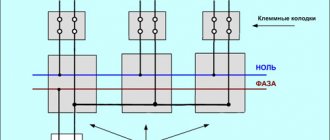
It is no secret that in a circuit any radio component, for example a microcircuit, can be connected by a huge number of conductors to other elements of the circuit. In order to free up space on the circuit diagram and remove “repetitive connecting lines,” they are combined into a kind of “virtual” harness—they denote a group communication line. In the diagrams, the group communication line is designated as follows.
Here's an example.
As you can see, such a group line is thicker than other conductors in the circuit.
To avoid confusion about which conductors go where, they are numbered.
In the figure I marked the connecting wire number 8 . It connects pin 30 of the DD2 chip and 8 of the XP5 connector. In addition, pay attention to where the 4th wire goes. For the XP5 connector, it is connected not to pin 2 of the connector, but to pin 1, which is why it is indicated on the right side of the connecting conductor. The 5th conductor is connected to the 2nd pin of the XP5 connector, which comes from the 33rd pin of the DD2 chip. I note that the connecting conductors with different numbers are not electrically connected to each other, and on a real printed circuit board they can be located in different parts of the board.
The electronic content of many devices consists of blocks. And, therefore, detachable connections are used to connect them. This is how detachable connections are indicated on the diagrams.
XP1 is a plug (aka "Male"), XS1 is a socket (aka "Female"). All together this is “Papa-Mama” or connector X1 ( X2 ).
Electronic devices may also contain mechanically coupled elements. Let me explain what we are talking about.
For example, there are variable resistors that have a built-in switch. I talked about one of these in the article about variable resistors. This is how they are indicated on the circuit diagram. Where SA1 is a switch and R1 is a variable resistor. The dotted line indicates the mechanical connection of these elements.
Previously, such variable resistors were very often used in portable radios. When we turned the volume control knob (our variable resistor), the contacts of the built-in switch first closed. Thus, we turned on the receiver and immediately adjusted the volume with the same knob. I note that the variable resistor and switch do not have electrical contact. They are only connected mechanically.
The same situation is with electromagnetic relays. The relay coil itself and its contacts do not have an electrical connection, but they are mechanically connected. We apply current to the relay winding - the contacts close or open.
Since the control part (relay winding) and the executive part (relay contacts) can be separated on the circuit diagram, their connection is indicated by a dotted line. Sometimes a dotted line is not drawn at all , and at the contacts they simply indicate the relay membership ( K1.1 ) and the number of the contact group (K1. 1 ) and (K1. 2 ).
Another fairly clear example is the volume control of a stereo amplifier. To adjust the volume, two variable resistors are required. But adjusting the volume in each channel separately is impractical. Therefore, dual variable resistors are used, where two variable resistors have one control shaft. Here is an example from a real circuit.
In the figure, I highlighted two parallel lines in red - they indicate the mechanical connection of these resistors, namely that they have one common control shaft. You may have already noticed that these resistors have a special position designation R4. 1 and R4. 2 . Where R4 is the resistor and its serial number in the circuit, and 1 and 2 indicate the sections of this dual resistor.
How to read datasheets
Datasheets, out of habit, frighten you with their volume and abundance of incomprehensible words. In fact, everything is not so scary if you know a few life hacks.
Install a good PDF reader . Datasheets are written in the glorious tradition of paper instructions; they are great to print out, insert with plastic bookmarks and sew. Hypertext in them is observed in trace quantities. Fortunately, at least the structure of the document is designed with bookmarks, so a suitable reader with easy navigation is very necessary.
The datasheet is not Stroustrup’s textbook; you don’t have to read everything . If you used the previous advice, just find the desired section in the bookmarks bar.
Datasheets, especially Reference Manuals, can describe the capabilities of not a specific chip, but the entire line . This means that half, or even two-thirds of the information is not relevant to your chip. Before exploring TIM7 registers, check the General Description to see if you have one.
to know English at a basic level . Datasheets consist half of terms unfamiliar to the average native speaker, and half of simple connecting structures. There are also excellent Chinese datasheets in Chinese English, where half are also terms, and the second half are a random set of words.
If you come across an unfamiliar word , do not try to translate it using an English-Russian dictionary. If you are perplexed by hysteresis, then the translation “hysteresis” will not make you any warmer. Use Google, Stack Overflow, Wikipedia, forums, where the required concept will be explained in simple words with examples.
The best way to understand what you read is to test it in action . Therefore, keep on hand the debug board that you are familiarizing yourself with, or better yet two, in case you still misunderstood something and saw a magic smoke.
It’s a good habit to keep a datasheet handy when you ’re reading someone’s tutorial or studying someone else’s library. It is quite possible that you will find a more optimal solution to your problem in it. And vice versa - if you can’t understand from the datasheet how the register actually works, google it: most likely, someone has already described everything in simple words or left clear code on GitHub.
How to learn to read an electrical diagram
Any radio equipment includes individual radio components that are soldered together using a certain method. All these elements are reflected on the electrical circuit with conventional graphic values. To learn how to read a document, you need to understand the symbols of all conductive elements of an electrical circuit. Each part has its own graphic designation and includes a conventional design with characteristic features.
The easiest way to work is with an element such as an electronic capacitor with resistors, speakers and other electrical equipment with automation. As a rule, they are easy to recognize without any table with symbols. It's easier to learn from them. It is more difficult to work with semiconductors, namely transistors, triacs and microcircuits. For example, each bipolar transistor has three terminals, namely, a base, a collector and an emitter. For this reason, conventional images and clarifying information in the form of Latin letters are necessary. Learning them can take many days, as can learning to recognize them.
Note! In addition to letters, each diagram has numbers. They talk about numbering and technical specifications. It is worth pointing out that it is impossible to learn to read a document on your own, and therefore lessons and tutorials are needed.
Basic Rules
In answer to the question of how to read electrical circuits, it is worth clarifying that this must be done from left to right, from beginning to the very end. This is the basic rule. The next rule is to divide a single drawing into small pictures or simple chains. It consists of an electric current source, a current receiver, a direct drive, a return wire and one contact of the device. Therefore, when starting to study a document, you need to break it into parts. Next, you must take into account all the details, with comments, explanations, explanations and specifications. If there are references in the drawing, then you need to study them too.
Note! Drawings that reflect the operation of the power supply, electrical protection, control and signaling must be studied for the number of power sources, interaction, consistency of teamwork, assessment of the consequences of probable faults, violation of wire insulation, checking the circuit with the absence of false circuits, assessing the reliability of the electrical supply, mode operation of equipment and checking the implementation of measures that ensure safe work.
Legend
According to regulatory documents, there are standard graphic symbols in one-line and two-line diagrams. The following is a table with similar symbols called electrical diagrams for beginners symbols. It is worth pointing out that numbers and letters are also used in the drawings. Such marking is regulated by regulatory documents, namely GOST.
Dictionary
Some useful words and symbols to help you quickly get used to datasheets. What I remembered in the last couple of days, additions and corrections are welcome.
Electricity Vcc , Vdd – “plus”, power supply Vss , Vee – “minus”, ground current – current voltage – voltage to sink current – work as “ground” for an external load to source current – power an external load high sink/source pin – pin with increased “tolerance” to load
IO H, High – on the Vcc L pin, Low – on the Vss High Impedance , Hi-Z , floating – there is nothing on the pin, “high resistance”, it is actually invisible to the outside world. weak pull up , weak pull down – built-in pull-up/pull-down resistor, approximately analogous to 50 kOhm (see datasheet). It is used, for example, to prevent the input pin from dangling in the air, causing false alarms. Weak - because it is easy to “beat”. push pull – pin output mode in which it switches between High and Low – regular OUTPUT from Arduino. open drain – designation of the output mode, in which the pin can be either Low or High Impedance / Floating. Moreover, almost always this is not a “real” open drain; there are protective diodes, resistors, and whatnot. This is simply a designation for ground/none mode. true open drain - but this is a real open drain: the pin leads directly to the ground if open, or remains in limbo if closed. This means that, if necessary, a voltage greater than Vcc can be passed through it, but the maximum is still specified in the datasheet in the Absolute Maximum Ratings / Voltage section.
Interfaces in series - connected in series to chain - assemble chips into a chain by serial connection, increasing the number of outputs. shift – shift, usually denotes a bit shift. Accordingly, to shift in and to shift out – receive and transmit data bit by bit. latch – a latch that covers the buffer while bits are shifted through it. When the transfer is completed, the valve opens and the bits begin to work. to clock in – perform a bit transfer, shift all the bits to the right places. double buffer , shadow register , preload register – designations of history, when the register should be able to accept new data, but hold it until some point. For example, for PWM to work correctly, its parameters (duty cycle, frequency) should not change until the current cycle ends, but new parameters can already be transferred. Accordingly, the current ones are kept in the shadow register, and the new ones end up in the preload register, being written to the corresponding register of the chip.
Any prescaler – frequency prescaler to set a bit – set a bit to 1 to clear/reset a bit – reset a bit to 0 (reset is a feature of STM datasheets) to toggle a bit – change the bit value to the opposite (see example at the beginning of the article)
What's next
In general, a practical part was planned here with a demonstration of three projects on STM32 and STM8, made specifically for this article using datasheets, with light bulbs, SPI, timers, PWM and interrupts:
But there is a lot of text, so the projects are sent to the second part.
The skill of reading datasheets will help you with your hobby, but it is unlikely to replace live communication with fellow hobbyists on forums and chats. For this purpose, you still need to improve your English first of all. Therefore, those who finished reading will receive a special prize: two free lessons in Skyeng with the first payment using the code HABR2.