Frequency converters are designed to smoothly regulate the speed of an asynchronous motor. This becomes possible by creating a three-phase voltage with variable frequency at the output of the converter itself. Vector control, which is common and perfect, allows you to adjust the frequency and voltage.
The frequency converter, working in tandem with an asynchronous motor, makes it possible to abandon the DC electric drive. Asynchronous electric motors have advantages, including:
- Simplicity of the device and its operation;
- Reliability of the design;
- More comfortable dimensions and weight;
- More power at lower cost.
However, asynchronous electric motors also have one significant disadvantage, which is associated with the difficulty of adjusting their speed. The rotation speed of the executive parts of the mechanisms can be adjusted using different devices, but all of them do not provide the desired result, and they are also uneconomical. Control by classical methods: varying the supply voltage, adding additional resistances, etc., was a big problem.
With the development and spread of technology, static frequency converters (SFCs) have emerged, which are very affordable. VHFs are modern and economically feasible devices for controlling asynchronous drives.
The main principle is that when the frequency of the supply voltage changes, it is possible to change the angular velocity of the magnetic field. This will ensure smooth speed control over a wide range, and the mechanical characteristics are significantly improved. It is worth noting that slipping of an asynchronous motor is not allowed, therefore, power losses will be very insignificant.
In order to achieve high energy performance, the frequency and input voltage must be changed simultaneously. This will improve power factor, efficiency, and also improve overload capacity.
Feasibility of use
The use of an adjustable electric drive in various technological operations has its own number of advantages. First of all, it is worth noting the significant energy savings due to the adjustment of certain technological parameters. For each type of device or entire system, there are its own characteristic parameters, by adjusting which you can achieve significant results.
The most impressive economic effect can be achieved by using a frequency converter at facilities where various volumes of liquid are transported. But at the moment, this method has not become widespread, and adjustment is carried out by traditional control valves or gate valves. In this case, the flow of substance during throttling will be restrained by a gate or valve, without doing any useful work. If you use an adjustable electric drive for the pump, it will be possible to set optimal values for pressure and flow. This will reduce energy consumption and losses of the transported substance itself.
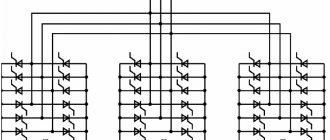
A significant part of the current static frequency converters is based on a double conversion circuit. The composition includes the following parts: DC links, control systems, power pulse inverter. The DC link includes an uncontrolled rectifier and a filter. AC voltage is converted to DC voltage.
The three-phase power pulse inverter is constructed from 6 transistor switches. Each of the electric motor windings is connected with a key to the appropriate output of the rectifier. The inverter, in turn, converts the previously rectified voltage directly into three-phase alternating voltage with the required frequency and amplitude.
Device
To convert one voltage level to another, pulse voltage converters using inductive energy storage devices are often used. According to this, three types of converter circuits are known:
- Inverting.
- Raising.
- Downgrades.
These types of converters have five elements in common:
- Key switching element.
- Power supply.
- Inductive energy storage (choke, inductor).
- A filter capacitor that is connected in parallel with the load resistance.
- Blocking diode.
The inclusion of these five elements in different combinations makes it possible to create any of the listed types of pulse converters.
Regulation of the output voltage level of the converter is ensured by changing the width of the pulses, which control the operation of the key switching element. Stabilization of the output voltage is created by the feedback method: a change in the output voltage creates an automatic change in the pulse width.
A typical representative of a voltage converter is also a transformer. It converts AC voltage of one value to AC voltage of another value. This property of a transformer is widely used in radio electronics and electrical engineering.
The transformer device includes the following elements:
- Magnetic core.
- Primary and secondary winding.
- Frame for windings.
- Insulation.
- Cooling system.
- Other elements (for access to winding terminals, installation, transformer protection, and so on).
The voltage that the transformer will produce on the secondary winding will depend on the turns that are present on the primary and secondary windings.
There are other types of voltage converters that have a different design. Their device in most cases is made on semiconductor elements, since they provide a significant efficiency.
Operating principle
The voltage converter generates the supply voltage of the required value from another supply voltage, for example, to power certain equipment from a battery. One of the main requirements for the converter is to ensure maximum efficiency.
Conversion of alternating voltage can be easily accomplished using a transformer, as a result of which such direct voltage converters are often created on the basis of an intermediate conversion of direct voltage to alternating voltage.
- A powerful alternating voltage generator, which is powered by an original direct voltage source, is connected to the primary winding of the transformer.
- An alternating voltage of the required magnitude is removed from the secondary winding, which is then rectified.
- If necessary, the constant output voltage of the rectifier is stabilized using a stabilizer, which is switched on at the output of the rectifier, or by controlling the parameters of the alternating voltage generated by the generator.
- To achieve high efficiency, voltage converters use generators that operate in switching mode and generate voltage using logic circuits.
- The output transistors of the generator, which switch the voltage on the primary winding, go from a closed state (no current flows through the transistor) to a saturation state, where the voltage across the transistor drops.
- In voltage converters of high-voltage power supplies, in most cases, self-inductive emf is used, which is created at the inductance in cases of sudden interruption of the current. A transistor acts as a current interrupter, and the primary winding of the step-up transformer acts as an inductance. The output voltage is created on the secondary winding and rectified. Such circuits are capable of generating voltages up to several tens of kV. They are often used to power cathode ray tubes, picture tubes, and so on. This ensures efficiency above 80%.
Kinds
Converters can be classified in a number of ways.
DC/DC converters:
- Voltage regulators.
- Voltage level converters.
- Linear voltage stabilizer.
AC/DC converters:
- Switching voltage stabilizers.
- Power supplies.
- Rectifiers.
DC to AC converters:
AC voltage converters:
- Variable frequency transformers.
- Frequency and voltage converters.
- Voltage regulators.
- Voltage converters.
- Transformers of various kinds.
Voltage converters in electronics, according to design, are also divided into the following types:
- On piezoelectric transformers.
- Self-generating.
- Transformer with pulse excitation.
- Switching power supplies.
- Pulse converters.
- Multiplexer.
- With switched capacitors.
- Transformerless capacitor.
How the device works
Let us next consider the principle of operation of the frequency converter under consideration.
A frequency converter with pulse-width control first equalizes the mains voltage using a diode bridge, and then it is smoothed and filtered by capacitors. And this is the first stage of transformation.
At the next step, using microcircuits and output bridge IGBT switches, a sequence of a specific duty cycle and frequency is formed from the DC voltage. Rectangular pulses are generated at the output of the frequency converter, but due to the inductance of the windings, they are integrated and converted into a voltage close to a sinusoid.
How to choose an HRO?
- by function. Most budget converters have only the most important functions, but there is competition among manufacturers, and therefore basic variations in their functionality can differ significantly.
- according to the control method. There are two options here: scalar and vector control. Vector is more modern, widespread and complex. Scalar is suitable for simple devices, and is cheaper.
- by power. If the power of the equipment is approximately equal, then you should choose converters from the same company based on the maximum load indicator.
- according to mains voltage. It is recommended to select a converter with the largest range of upper and lower values.
- according to the frequency adjustment range. Depending on the operating frequencies of the drive and focusing on the maximum permissible values, you should select a converter with a suitable frequency range.
Menu
Currently, among the problems solved with the help of converter technology, a large place is occupied by those associated with the operation of a powerful converter at low supply voltages and high currents. A typical example of such a converter is the operation of the converter as part of autonomous power supply systems when receiving primary electrical energy from a low-voltage source (chemical current sources, in particular, hydrogen fuel cells, thermogenerators, etc.). For a number of such applications, an important indicator is efficiency, an increase in which can also help reduce the weight and dimensions of the device. There are known circuit solutions used in the construction of high-current low-voltage converters. A circuit with a transformer midpoint output is widely used. The advantage of the circuit is the inclusion of only one key in the power current circuit. The latter determines small static losses in the semiconductor elements of the circuit, which are fundamental in such applications.
A significant disadvantage of the scheme is the complex design of the transformer, the installed power of which increases due to the inefficient use of the primary winding. In addition, in the basic circuit there are no ways to output the energy of the leakage inductances of the windings. When this energy is dissipated, the efficiency of the converter decreases significantly. The corresponding dependencies are shown in Fig. eleven]. To increase efficiency, the circuit includes additional elements designed to output this energy to the load or power source, if such a possibility is allowed. For example, in Fig. Figure 2 shows a circuit with an additional converter for outputting the energy accumulated in leakage inductances to the primary source [1]. However, such modification complicates the operating mode and design of the converter. Converters are characterized by pulsed consumption and pulsed transfer of energy to the load.
Noticing that converters with a closed input [2] are characterized by a continuous current consumption, it was proposed to build converters on the principle of converters with a closed input and free exchange of energy between the internal circuits and the power source.
The proposed approach makes it possible to strictly control the voltage on the circuit elements at a level greater than or equal to the supply voltage, ensures smooth current consumption by the converter, unambiguous control characteristics up to the idle mode, and eliminates the issue of controlling the energy accumulated in the transformer leakage inductances.
One of the circuit options that implements this approach is shown in Fig. 3. Free exchange of energy between the internal circuits (inverter load VT1–VT4, capacitor) and the power source is ensured due to the fact that the control of biconducting switches on transistors VT1–VT4 is constructed in such a way that any pair of switches is turned on at any time. This ensures electrical communication between the internal circuits of the converter and the power source, regardless of the direction of the currents in the circuit.
Operation of the circuit Fig. 3 is illustrated by timing diagrams in Fig. 4. At the same time, we believe that semiconductor devices seem to be ideal switches, there are no losses in the circuit elements, voltage ripples on capacitor C are equal to zero, the load current is ideally smoothed, and the pulsating currents of reactors L1, L2 are continuous.
Four intervals can be distinguished in the operation of the circuit.
In the interval t0 – t1 (Fig. 4), transistors VT1 and VT4 are open. In this case, the reactor current L1 increases, closing along the circuit: +E, L1, VT1, –E. Using VT4, capacitor C is connected to the input of the rectifier VD5–VD8, and a voltage pulse is formed at the load, the amplitude of which is equal to the voltage across the capacitor. The load current in this interval is closed along the circuit: C, VT4, VD8, ZН, VD5, VT1, C. The reactor current L2 in this interval is closed along the circuit: +E, L2, VT4, C, –E. Thus, a current flows through capacitor C and transistor VT4 equal to the difference between the load current and the reactor current L2. As will be shown below, the load current is always greater than or equal to the current of the reactor L2, and the voltage on the capacitor C is greater than or equal to the supply voltage E. Under these conditions, the current of the transistor VT4 is always significantly less than the load current or even equal to zero. Thus, transistor VT4 is a lightly loaded element, and accordingly, energy losses in it are small. The most loaded element is transistor VT1, through which the reactor current L1 and the load current are closed.
In the interval t1–t2, transistor switches VT3, VT4 are open. These can be diodes VD3, VD4, or these diodes are shunted with open transistors to increase efficiency. The currents of the reactors L1, L2 flow into capacitor C (Fig. 4b), falling under the influence of the difference in voltage across the capacitor and the supply voltage. At this interval, a zero pause is formed at the load (Fig. 4d).
In the interval t2 – t3, transistors VT2 and VT3 are open, a voltage pulse is formed at the input of the rectifier VD5–VD8 with parameters similar to the parameters of the pulse in the interval t0 – t1, but of opposite polarity (Fig. 4a). The interval t3–t4 is similar to the interval t1–t2.
We will analyze the electromagnetic processes in the circuit under the assumptions made above.
For the continuous reactor current mode, we can write the following expression for the reactor current i1 over the pulse interval:
where Imin is the minimum value of the reactor current; L1 = L2 - reactor inductance; E—supply voltage; ti = t1 – t0 is the duration of the voltage pulse on the load (Fig. 4d), equal in this mode to the duration of the conducting state of the switch VT1 (tprVT1) or VT2 (tprVT2) with symmetrical control tprVT1 = tprVT2 = tpr.
In the interval T – ti = t4 – t1, when transistor VT1 is closed (Fig. 4), the reactor current i2 decreases according to the law
where Imax is the maximum value of the reactor current; UC is the voltage across capacitor C; T is the operating period of the circuit.
Considering that i1(tu) = Imax, i2(T – tu) = Imin, we solve (1) and (2) together and obtain
where γ* = tpr/T = tu/T is the relative duration of the conducting state of the switches VT1 and VT2, equal in this mode to the relative duration of the pulse on the load.
During the operation period of the circuit T, two pulses of duration ti are formed at the load (Fig. 4). Then the average value of the desired voltage across the load is:
Note that expression (4) is valid only for the case 0 ≤ γ* ≤ 0.5. At γ* = 0.5, the pause in the output voltage is zero (Fig. 4d).
If γ* > 0.5, the shape of the output voltage changes (Fig. 5). In this case, a pause again appears in the output voltage due to the interval of jointly conducting transistor switches VT1, VT2. In this case, the duration of the pause on the load is equal to tP = tpr – T/2, and the duration of the pulse on the load is equal to T/2 – tP. The average value of voltage across the load at γ* > 0.5 is:
Thus, at γ* > 0.5, the output voltage at the load is constant and equal to 2 E. However, the voltage on the capacitor and on other circuit elements increases in accordance with expression (3). Consequently, changing the relative pulse duration γ* in the range γ* > 0.5 is irrational in this application and is not considered further by us.
With the symmetry of the power elements and control, a strictly symmetrical (without a constant component) voltage is formed at the input of the rectifier VD5–VD8. Then, to ensure potential decoupling and matching the given level of input and output voltage, the circuit can be supplemented with a matching transformer installed at the input of the rectifier VD5–VD8, with a given transformation ratio Ktr = ω2/ω1, where ω1 is the number of turns of the primary winding, ω2 is the number of turns secondary winding. By introducing a new relative duration of the conducting state of the keys VT1, VT2 γ, equal to
Let us transform expressions (3) and (4) in the general case, taking into account the ideality of the matching transformer, to the form:
Accepted? changes in the range 0 ≤ γ ≤ 1, while γ* changes in the range 0 ≤ γ* ≤ 0.5. The average value of the consumed current IВХ can be found from the energy balance condition. When the efficiency of the circuit is equal to unity (η = 1),
from where, taking into account (8), we get
In a symmetrical circuit, the currents of reactors IL1 and IL2 are equal to each other and equal to half of the consumed current
The ripple range of the consumed current can be estimated based on the following considerations. In a lossless circuit in steady state, the increment in input current during the pulse interval (ti = t1 – t0 Fig. 4) is equal to the value of the current decay during the pause (t1 – t2) and is determined by the total increment in the current of reactors L1 and L2.
Taking into account expression (7) and the equality tи = t1 – t0 we obtain
where ƒ = 1/T, L = L1 = L2.
In this case, the pulsation frequency ƒP is twice as high as the operating frequency of the circuit ƒ. Expression (12) shows that when γ = 1 (the highest load of the converter), there is no ripple in the consumed current, the converter consumes an ideally smoothed current. The ripple factor of the consumed current is equal to
The maximum and minimum current consumption is:
Let's find the limit value of the load current IН ГР, at which the currents of the chokes L1 and L2 become discontinuous or alternating. The latter depends on the method of controlling transistors VT3 and VT4. For this current, using (1), we can write i1(tu) = Imax = 2IL1 at Imin = 0. Therefore, taking into account (9), we can obtain:
If during a pause transistors VT3 and VT4 are turned off, then at IN < IN GR the currents become discontinuous. If transistors VT3 and VT4 are switched on during a pause, then at IN < IN GR the inductor currents change sign. The latter means that the energy accumulated in the reactive elements of the circuit is partially returned to the power source during a pause. This ensures free exchange of energy in the circuit. The continuous current mode is observed in this case, and the above expressions for voltage UC remain valid for the mode IN < IN GR.
The average current value of transistor switches VT1 and VT2 is determined by the sum of the load current and the reactor current over the pulse interval (ti = t1 – t0). Taking into account (1) we obtain:
where Imin = IL – ΔIL/2 – minimum current of one reactor, IL, ΔIL – average value and current increment over the pulse interval of one reactor.
Noticing that
and taking into account (10), finally for the current of switches VT1 and VT2 we obtain
By the average value of the current of keys VT3, VT4 we mean the average absolute value of the current of these keys. This is explained by the fact that regardless of which element of the switch (transistor or diode) the current is closed, it will characterize the total losses in the switch, the installed power of the switch, etc. At pause intervals (t1 - t2), (t3 - t4) through the switch diode VD3, the reactor current L1 is closed; during the pulse interval (t2 - t3), the difference between the load current and the reactor current L1 is closed through the switch transistor VT3. In this case, expression (10) shows that the reactor current (with sufficiently small ripples of this current) is always less than or equal to the load current, converted to the primary winding. Therefore, for the average absolute value of the current of the switch VT3 (in a symmetrical circuit, the current of the switch VT3 is equal to the current of the switch VT4) can be written, taking into account (10):
Expression (19) shows that with γ tending to unity (highest power mode in the load), the current of switches VT3 and VT4 with sufficiently small ripples of the reactor current practically tends to zero. It is easy to show that the largest average absolute value of the current of switches VT3 and VT4 is achieved at γ = 0.586 and is equal to:
Having designated the range of voltage ripples on capacitor C as ΔUC, and noting that during the pause intervals (t1 – t2), (t3 – t4) the input current IВХ flows through the capacitor, we can write:
Solving (21) together with (9), we obtain an expression for determining the value of the capacitor C at a given ΔUC:
The capacitance value of the capacitor at a given ΔUC is selected taking into account the fact that the maximum voltage ripple on the capacitor occurs at γ = 0.586. Therefore, the selected capacitance value of the capacitor is equal to:
It should be noted that the voltage ripple frequency on the capacitor ƒPS is equal to twice the operating frequency of the circuit ƒ, therefore expression (22) can be written as follows:
where ƒPS is the voltage ripple frequency on the capacitor.
Using the expressions obtained above, you can estimate the operating parameters of the circuit elements and calculate the characteristics of the converter. The main characteristics of the converter are shown in Fig. 6, 7, 8, 9 in relative units. The figures indicate points obtained when testing a prototype converter powered by a voltage of 24 V with an output power of 2 kW.
In Fig. Figure 10 shows the dependences reflecting the relative voltage on the switches of the circuit under consideration, operating in the output voltage stabilization mode, when the supply voltage changes. The x-axis shows the multiplicity of change in supply voltage E* = E/Emin, where Emin is the minimum supply voltage. The ordinate axis shows the factor of change in the maximum voltage on the switches Ukl* = Ukl/Uklmin, where Uklmin is the minimum voltage on the switches (provided that at γ = 1 the supply voltage E = Emin). It can be shown that for the circuit in Fig. 3 Ucl = (E* + 1)/2. The same graph shows a similar relationship typical for a bridge circuit and a transformer midpoint circuit. For these schemes, obviously, Ucl* = E*. As can be seen from the graphs, the higher the multiplicity of change in supply voltage, the more advantageous is the use of the circuit in question in the stabilization mode.
Analyzing the obtained dependencies, we can draw the following conclusions:
- The circuit consumes continuous current with low ripple in all modes. The ripple of the consumed current is always significantly less than the ripple of the current of any of the input reactors.
- The voltage on the load circuit during a pulse is always higher than the supply voltage and equal to the voltage on capacitor C. The latter makes it possible to reduce the transformation ratio of the matching transformer in step-up converters, which makes this circuit especially promising when powered from low-voltage sources.
- The fundamental feature of the circuit is that the power current is actually closed through one of the lower transistors VT1 or VT2, transistors VT3 and VT4 are lightly loaded, in the limit at γ ≈ 1, the currents of the switches VT3 and VT4 are practically equal to zero, which increases the efficiency of the circuit, especially with low-voltage power supply, when the determining losses are static losses in the switches.
- Regulation of the output voltage in the circuit is carried out not only due to the duty cycle γ, but also due to changes in the amplitude of the output pulses during the regulation process. Moreover, if this circuit is used in the mode of stabilizing the output voltage when the supply voltage changes, then the voltage level on the circuit elements, other things being equal, turns out to be lower than in circuits in which stabilization is carried out only due to the duty cycle γ (for example, a circuit with an output midpoint of the transformer).
To assess the prospects for using the proposed circuit solution, we will conduct a comparative analysis of power losses in semiconductor devices of the inverter part of the circuit in Fig. 3 and those that have found the greatest application in converter technology are converters built on the basis of a bridge circuit and a circuit with a transformer midpoint output (Fig. 11).
Let us assume that the compared circuits use the same type of power MOS transistors. The supply voltage (E) and load voltage (UN) are the same in all circuits. The load current is ideally smoothed, the active component of the load (RN) is the same. The latter means that the same power is released in the load. We will calculate the switch currents in the compared circuits under the condition that there are no losses in the circuits, in fact, we assume that losses in the switches have little effect on the current distribution in the compared circuits. We will assume that the compared circuits are used as boost DC/DC converters.
The voltage across the load of the bridge and zero circuits can be found from the expression
where Ktr = ω2/ω1 - transformation ratio; ω1 is the number of turns of the primary winding of a bridge circuit transformer, or half of the primary winding of a transformer in a circuit with a transformer midpoint output; ω2 is the number of turns of the secondary winding of the transformer; γ1—fill factor.
Voltage across the circuit load Fig. 3 is determined by expression (8). Note that with the same supply voltage and load voltage, in the general case,
The load voltage in the compared circuits reaches its maximum under the condition γ = γ1 = 1. Then from expressions (8) and (25) we obtain that
provided that the maximum voltage in the circuits is equal.
When the load current (IN) in the circuits is equal, the current of the primary winding of the transformer, which is the load current of the inverters during the pulse in the bridge and neutral circuits, is twice as large as in the circuit in Fig. 3. Further, for simplicity, we will assume that Ktr = 1. Taking into account the above, we can estimate the conductivity losses of the transistor in the bridge and zero circuits (PM, O).
where T is the operating period of the inverters; rON is the resistance of the transistor in the conducting state.
Dynamic losses in bridge and neutral circuit transistors will actually be determined by turn-off losses, since turn-on losses in these circuits are relatively small. The latter is determined by the fact that the turn-on time of the MOS transistor is significantly less than the switching time of the current from the diodes of the output rectifier to the transistor, due to the leakage inductance of the matching transformer. In this case, the transistor turns on at a low current.
Using the technique for estimating switching losses [3], for a bridge circuit transistor we obtain an expression that determines the switching losses (Poff.m.):
where Ucl = E is the voltage across the transistor; Icl = 2 × IN — transistor current; toff — transistor turn-off time; ƒ is the switching frequency of the transistor, equal to the operating frequency of the bridge circuit.
For a circuit with a midpoint of the transformer, switching losses (Pav. avg) are equal to
where Ucl = 2 × E is the voltage on the transistor at the moment of switching off.
The total losses in semiconductor devices of the bridge circuit (Pbridge), taking into account (27) and (28), are equal
The total losses in the semiconductor elements of the circuit with the midpoint of the transformer (Paverage) are equal, taking into account (27) and (29)
In the diagram of Fig. 3 conduction losses in transistors VT1 and VT2 are determined by the sum of the load current and the current of the corresponding input reactor. Taking into account (10), we find the effective value of the current of the transistor switches:
The direct conduction losses in the indicated transistors are equal to
The effective value of the current in transistors VT3 and VT4 during the pulse interval is determined by the difference between the load current and the reactor current, and during the pause interval - by the reactor current. Taking into account the notation (Fig. 4) and expression (10) for the effective value of the transistor current, we obtain:
The direct conduction losses in the indicated transistors are equal to
In Fig. 12 shows in relative units the dependence of the effective current values through switches VT1 and VT3 on the fill factor γ, constructed using the expressions obtained above.
The switching losses of transistors VT1 and VT2 are determined only by the reactor current (10) and the voltage on capacitor C (7) and do not depend on the load current. The latter is explained by the fact that the switching time of the load current from the diodes of the output rectifier is much longer than the switching time of the transistors, thereby the influence of the load current on the switching losses is insignificant, similar to how it was taken into account in the circuit with the output of the transformer midpoint and in the bridge circuit. The turn-off losses are determined by the sum of the reactor and load current and the voltage at C. Using the method [3], we obtain for the total dynamic losses in transistors VT1 and VT2:
where ton is the turn-on time of the transistor.
The switching losses of VT3 and VT4 are low because the transistors turn on and off at zero voltage.
Taking into account (33), (35) and (36), we obtain an expression for determining losses in the semiconductor elements of the circuit in Fig. 3:
Where
If the load voltage is equal during the regulation process, taking into account (8), (25) and (26), it is easy to show that
Then, taking into account that IH = UH/RH, and replacing γ1 with γ in (30) and (31), we obtain:
Expressions (39), (40) and (41) allow you to calculate the losses in the transistors of the compared circuits operating at the same input and output voltages for an identical load. In Fig. Figure 13 shows the dependence of losses in semiconductor circuit elements when regulating the output voltage. Losses are calculated at E = 24 V, Ktr = 1, RN = 0.48 Ohm, ƒ = 30 kHz, rON = 5·10-3 Ohm, toff = 120 ns, ton = 50 ns.
Comparing the obtained dependencies, you can see that the diagram in Fig. 3 is similar in transistor losses to the midpoint transformer circuit, and both circuits are significantly better than the bridge circuit under given conditions. Identicality in losses of the circuit with the output of the midpoint of the transformer and the circuit in Fig. 3, despite the fact that in the diagram of Fig. 3 there are additional transistors (VT3, VT4), flowing current, which can be explained based on the following physical considerations. Current amplitude in transistors VT1, VT2 circuit Fig. 3 under the condition of ideally smoothed reactor currents and load and circuit symmetry is equal, taking into account (10):
The current amplitude in the transistors of the circuit with the output of the transformer midpoint is equal to
However, the relative pulse duration in the circuit with the output of the middle point of the transformer γ1, other things being equal, is less than the relative pulse duration γ in the circuit in Fig. 3, since in the diagram of Fig. 3, the output voltage is regulated not only by γ, but also by changing the voltage amplitude across the load, proportional to the voltage across capacitor C (7). The current amplitude in VT1 and VT2, as can be seen from (42), decreases with decreasing relative pulse duration γ. However, due to the fact that the relative pulse duration γ is greater than the relative duration γ1, current flows through VT1 and VT2 of the circuit in Fig. 3 for a time greater than the duration of the conducting state of the keys in the circuit with the output of the transformer midpoint. In addition, transistors VT3 and VT4 circuits in Fig. 3 flow around a small difference current if the relative pulse duration γ is less than unity. These factors determine almost the same dependence of losses on the relative pulse duration in the circuit with the output of the transformer midpoint and in the circuit in Fig. 3.
At the same time, the diagram in Fig. 3 has a matching transformer, simpler in design, with a lower transformation ratio and lower installed power. The circuit consumes a well-smoothed current. In some applications, for example, in load voltage stabilization mode, it is possible to use devices with a lower permissible voltage. All of the above favorably distinguishes the proposed circuit from known technical solutions, especially in the field of low supply voltages and high currents.
Using the proposed approach to construction, it is possible to implement a number of circuits that have additional advantages compared to the circuit in Fig. 3.
In Fig. 14 is a circuit which may be called a split-capacitor circuit, which has the same advantages as the circuit in Fig. 3, providing parametric equalization of voltage half-waves on the transformer and eliminating magnetization of the transformer in case of asymmetry of control or circuit parameters.
In case of control asymmetry, when the duration of the positive pulse on the primary winding of the transformer is not equal to the duration of the negative pulse, the amplitudes of these pulses, equal to the voltages on the capacitors C1 and C2, are also not equal. In this case, during pauses (VT3 and VT4 are open), a voltage difference across the capacitors is applied to the primary winding of the transformer (Fig. 15).
Noting that for γVT1 ≠ γVT2, where γVT1 = (2 × tprVT1)/T and γVT2 = (2 × tprVT2/T) are the filling factors of VT1 and VT2, respectively, we determine the voltage on the capacitors:
If γVT1 < γVT2, then UC1 < UC2, then the area of the positive voltage half-wave is equal to:
Dividing the left and right sides by T/2 and taking into account (44), we obtain
The area of the negative half-wave divided by T/2 is equal to:
The equality of expressions (46) and (47) proves the validity of the statement about the parametric balancing of the transformer operating mode.
Naturally, with asymmetrical control, the frequency of the first harmonic of the output voltage ripple is two times lower than in a symmetrical circuit.
The approach used to construct the circuit described above can be successfully applied to construct multiphase circuits. In Fig. Figure 16 shows a diagram of a three-phase DC/DC converter. It is characterized by the use of three input chokes, three capacitors and three transistor half-bridges, which form the arms of a three-phase bridge circuit. In this case, you can use a multiphase (in this case three-phase) transformer, which makes it possible to reduce its weight and dimensions at the same installed power. The supply of control pulses to the transistors is carried out with a phase shift between the control pulses of different half-bridges. Voltage oscillograms explaining the operation of the circuit in Fig. 16 are shown in Fig. 17.
Similar to the single-phase circuit discussed above, for multiphase circuits there is a maximum pulse interval duration, above which the average voltage across the DC/DC converter load does not change, but only the pulse amplitudes change. Let us denote the ratio of the duration of the open state of the lower transistors (in Fig. 16 - transistors VT1, VT3, VT5) to the operating period of the circuit γ*. It can be shown that the indicated maximum duration of the open state of the lower key corresponds to γ*max = (m – 1)/m, where m is the number of phases (for the circuit in Fig. 16 m=3), γ*max = (m – 1)/ m = 2/3. The phase shift between the pulses supplied to the phase arms corresponds to a time shift of 1/m × T, where T is the operating period of the circuit. For the diagram in Fig. 16 this value is equal to T/3.
The regulating characteristic of such a circuit has two sections, depending on γ* (Fig. 18).
The voltages on the capacitors, similarly to (3), are determined by the relation:
At the maximum value of γ* = 2/3, the voltage on the capacitors is three times greater than E, and thus the voltage amplitude on the primary winding is also three times greater than the supply voltage.
Let γ* < 1/3. With such a fill factor, there are intervals during which one lower key and two upper ones are closed (the duration of such an interval for each key is T×γ*), and intervals during which all upper keys are closed. Voltage is applied to the rectifier load only at intervals when the lower switch is closed. One of the linear voltages on the primary windings of the transformer is zero, and the other two are equal in absolute value to the voltages on the capacitors. Thus, taking into account that, generally speaking, the value of the voltage rectified by the rectifier on the secondary side is determined by the circuits for connecting the primary and secondary windings (“star-star”, “triangle-star”, etc.), which can be reflected by the coefficient KСХ, in circuit has three arms, for the average load voltage we can write:
Let now 1/3 ≤ γ* ≤ 2/3 (see Fig. 17). With such a duty cycle, there are intervals during which one lower key and two upper ones are closed (t1 – t2, t3 – t4, t5 – t6). There are also intervals during which one upper key and two lower ones are closed (t0 – t1, t2 – t3, t4 – t5). Both in the first and second time intervals, linear voltages are applied to the primary windings of a three-phase transformer, one of which is zero, and the other two are equal in absolute value to the voltages on the capacitors. On the secondary side of the transformer, therefore, there is always a voltage present, determined by the transformed voltages on the capacitors. This voltage is the same in absolute value, and only the phases involved and the polarity of the voltage on them change.
Therefore, the control characteristic can be written as follows:
The corresponding dependencies are shown in Fig. 18.
Multiphase circuits, and, in particular, this one, have all the advantages inherent in the single-phase circuit discussed above. In addition, they have additional unique advantages.
In a certain range of duty cycles γ* - from 1/m to (m-1)/m (for the circuit in Fig. 16 from 1/3 to 2/3) - the voltage at the rectifier load has no pauses between pulses, and with a change in the coefficient filling, only the amplitude of the pulses changes. That is, a constant voltage of a controlled value is supplied to the rectifier load. In addition, when the load voltage is stabilized when the supply voltage changes, the maximum voltage on the converter switches does not change and remains the same as at the minimum supply voltage. Due to this, the need to ensure the operation of the converter with a changing supply voltage and stabilize the load voltage does not require an increase in the class of the key devices used compared to the case of operation from a minimum supply voltage.
These advantages are explained by the fact that, as indicated above, in the indicated range either one or two lower keys are always closed. Therefore, regardless of the operating interval, the two line-to-line voltages are always non-zero and equal to the voltages on the capacitors. The output voltage is also always different from zero and is determined by the transformed voltage of the capacitors. When stabilizing the load voltage, it is necessary to maintain the same voltage on the capacitors, which determines the constancy of the voltages on the switches.
The inverter circuits on which the proposed circuit solutions for DC/DC converters are based can also be used as independent circuits designed to power an AC load. They can perform pulse width control and pulse width modulation.
Thus, the proposed approach makes it possible to construct circuit solutions that have the following advantages:
- smooth current consumption over a wide range of duty cycles;
- on the primary side of the matching transformer, the voltage is greater than the supply voltage, which reduces the transformation ratio in step-up converters, simplifies the design of the transformer (compared to a circuit with a transformer midpoint output) and reduces its parasitic parameters;
- when the load voltage stabilizes and the supply voltage increases, the maximum voltage on the switches and other elements of the converter circuit grows significantly more slowly than the supply voltage; due to this, the class of devices used is reduced;
- of the two key devices that make up the arm of the circuit, one is significantly unloaded in current, and only one switch of the pair makes a significant contribution to the losses in the semiconductor elements of the circuit, which can significantly increase the efficiency of the circuit;
- the energy accumulated in the leakage inductance of the transformer during the pulse is automatically transferred to the load or primary power source, which does not require any changes or additions to the circuit;
- the circuit is resistant to asymmetry, which can be asymmetry of control or asymmetry of the parameters of key elements of the circuit, etc.
Polyphase circuits also have the following unique advantages:
- in a certain range of duty cycles, the rectifier load is supplied with a constant, zero-ripple, voltage of an adjustable value; with appropriate control of the upper switches of the circuit arms, unambiguous adjustment characteristics are provided up to the idle mode;
- when the load voltage stabilizes when the supply voltage changes, the maximum voltage on the converter switches remains the same as at the minimum supply voltage; Due to this, the need to ensure the operation of the converter with a changing supply voltage and stabilization of the load voltage does not require an increase in the class of the key devices used compared to the case of operation from a minimum supply voltage.
Literature
- Tsarenko A. I., Seregin D. A. On the issue of constructing powerful DC/DC converters powered from low-voltage networks // Power Electronics. 2006. No. 3.
- Handbook of converter technology / Ed. I. M. Chizhenko. K.: Technology. 1978.
- Williams B. Power electronics: devices, application, control. Reference manual: translation from English. M.: "Energoatomizdat". 1993.
General conclusions
An asynchronous motor equipped with a squirrel-cage rotor is by far the most reliable and widespread device. But, despite numerous advantages, this type of engine also has significant disadvantages. For example, this is the lack of ability to vary the rotor speed and a fairly serious starting current, which is 5-7 times higher than the rated current.
In the case where only mechanical control devices are used, the above-mentioned disadvantages can lead to significant energy losses and mechanical shock loads. Such phenomena have an extremely negative impact on the durability of the equipment.
The solution to such problems was not the traditional mechanical, but an innovative electronic method. A frequency converter with pulse-width control can reduce inrush currents by four to five times. It ensures a smooth start of an asynchronous motor, and also controls the drive using a given voltage and frequency ratio.
The frequency converter makes it possible to save up to fifty percent of energy. In addition, it is possible to enable feedback among the drives, which allows the equipment, if necessary, to adjust itself independently.
Static electromagnetic converter…