Device and principle of operation
A transistor is an electronic semiconductor consisting of 3 electrodes, one of which is the control one. A bipolar type transistor differs from a polar one in the presence of 2 types of charge carriers (negative and positive).
Negative charges are electrons that are released from the outer shell of the crystal lattice. A positive type of charge, or hole, is formed at the site of the released electron.
The design of a bipolar transistor (BT) is quite simple, despite its versatility. It consists of 3 conductor-type layers: emitter (E), base (B) and collector (K).
An emitter (from the Latin "to release") is a type of semiconductor junction whose main function is to inject charges into the base. The collector (from the Latin “collector”) serves to receive emitter charges. The base is the control electrode.
The emitter and collector layers are almost identical, but they differ in the degree of addition of impurities to improve the characteristics of the PCB. Adding impurities is called doping. For the collector layer (CL), doping is weakly expressed to increase the collector voltage (Uc). The emitter semiconductor layer is heavily doped in order to increase the reverse permissible breakdown U and improve the injection of carriers into the base layer (the current transfer coefficient - Kt increases). The base layer is lightly doped to provide greater resistance (R).
The junction between base and emitter is smaller in area than KB. Thanks to the difference in areas, the CT improves. When the PP is operating, the K-B junction is switched on with a reverse bias to release the bulk of the amount of heat Q, which is dissipated and provides better cooling of the crystal.
The performance of BT depends on the thickness of the base layer (BL). This dependence is a quantity that varies in inverse proportion. Less thickness means faster performance. This dependence is related to the time of flight of charge carriers. However, this reduces Uk.
What it is
A transistor is a special semiconductor-type electrical circuit element that serves to change the basic electrical parameters of an electric current and to regulate these parameters. In a standard semiconductor triode there are only 3 outputs: a collector, a charge injector and a base element, to which the electrons from the control are actually sent. There are also combined transistors with high power. While typical elements used in integrated circuits can be a few nanometers in size, production transistors for industrial plants are packaged and are up to 1 centimeter wide. The reverse voltage of production control triodes reaches 1 thousand Volts.
2SD1710 for switching power supplies
The triode design is made on the basis of semiconductor layers enclosed in the element body. Semiconductors are materials based on silicon, germanium, gallium and some other chemical elements. Currently, many studies are being conducted that propose various types of polymers and carbon nanotubes as materials.
Important! Once upon a time, semiconductor crystals were housed in metal compartments in the form of hats with three terminals. This structure was typical for transistor-type point elements.
Various types of radioelements under consideration
Today, the structure of almost all planar and silicon transistors is based on a doped single crystal. They are in plastic, metal or glass cases. Many of them have protruding leads to help dissipate heat when the electricity gets too hot.
Silicon bipolar transistor 2SA1286
The terminals of modern transistors are usually located in one row. This is convenient, since the board is assembled by robots, and this saves resources. The output contacts are also not marked on the element body. The type of output is determined according to the operating instructions or after test measurements.
You may be interested in Features of the S1-67 oscilloscope
Important! For transistors, semiconductor alloys with different structures are used: PNP or NPN. Their difference lies in the different voltage signs at the terminals.
If we take it schematically, this radio element can be described as follows: two semiconductors separated by an additional layer that controls the conductivity of the triode.
Diagram of the device of field radio elements
Operating modes
A bipolar transistor can operate in 4 modes:
- Active.
- Cutoffs (RO).
- Saturation (RN).
- Barrier (RB).
The active BT mode is normal (NAR) and inverse (IAR).
Normal active mode
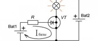
In this mode, U flows at the E-B transition, which is direct and is called the E-B voltage (Ue-b). The mode is considered optimal and is used in most schemes. Transition E injects charges into the base region, which move to the collector. The latter accelerates the charges, creating an amplification effect.
Designation on electrical circuits
The transistor has an accepted designation: “VT” or “Q”. After the letters you need to indicate the position index. For example, VT 2. On old drawings you can find symbols: “T”, “PP” or “PT”, which are no longer used. The transistor is drawn in the form of certain segments indicating the electrode contacts. Sometimes they are circled. The direction of the electric current in the emitter area is indicated by a special arrow.
Scheme of operation of the simplest radio element
Based on their operating principle and structure, the following semiconductor triodes are distinguished:
- Field type;
- Bipolar;
- Combined.
They all have similar functionality and differ in operating technology.
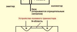
Field
Such triodes are also called unipolar, because of their electrical properties - they flow current of only one polarity. This type is also divided into several types according to its structure and type of adjustment:
- Transistors with PN control transition;
- Elements with an insulated shutter;
- The same transistors of a different structure (metal-dielectric-conductor).
Important! An insulated gate has one distinctive feature - the presence of a dielectric layer between it and the channel.
Diagram of an element with an insulated gate
Another feature of field-effect transistors is low power consumption. For example, such an element can function for more than one year on one battery. Field radio elements are quite independent: they consume extremely little electricity. Such a device can operate for years on a AA battery or a small battery. This is what led to their widespread use in electrical circuits and devices.
You may be interested in Installing a surge arrester
Electron-hole transition
Bipolar
These elements got their name because they are capable of passing plus and minus electric charges through one passage channel. They also have low input impedance. Such devices work as signal amplifiers and switches. Thanks to them, you can connect a fairly strong load to the electrical circuit and reduce the effect of its resistance. Bipolars are the most popular active-type semiconductor devices.
The principle of operation of a bipolar transistor in a circuit
Combined
Combined elements are invented in order to achieve the required electrical parameters using one discrete state. They are:
- Bipolar with resistors embedded in their circuit;
- Two triodes of one or more structure structures in a single part;
- Lambda diodes - a combination of two field control triodes that create resistance with a minus sign;
- Elements in which field components control bipolar ones.
Combination transistor
Connection schemes
To correctly use and connect BTs, you need to know their classification and type. Classification of bipolar transistors:
- Materials of manufacture: germanium, silicon and gallium arsenide.
- Manufacturing features.
- Power dissipation: low power (up to 0.25 W), medium (0.25-1.6 W), high power (above 1.6 W).
- Limit frequency: low-frequency (up to 2.7 MHz), mid-frequency (2.7-32 MHz), high-frequency (32-310 MHz), ultra-high-frequency (more than 310 MHz).
- Functional purpose.
The functional purpose of BT is divided into the following types:
- Low-frequency amplification with normalized and non-standardized noise figure (NiNNKSh).
- High-frequency amplification with NiNNKSh.
- Micro-frequency amplification with NiNNKSh.
- Powerful high-voltage amplifiers.
- Generator with high and ultra-high frequencies.
- Low-power and high-power high-voltage switching switches.
- Pulse powerful for working with high U values.
In addition, there are the following types of bipolar transistors:
- P-np.
- Npn.
There are 3 circuits for switching on a bipolar transistor, each of which has its own advantages and disadvantages:
- General B.
- General E.
- General K.
Common emitter circuit
Very often, a transistor is characterized by characteristics corresponding to the circuit shown in Fig. 1.59. This circuit is called a common emitter circuit because the emitter is the common electrode for the voltage sources.
For this circuit, the input characteristic is the dependence of the current ib on the voltage ube at a given voltage uke, i.e. a dependence of the form ib= f (ube) |u ke = const, where f is a certain function.
The output characteristic is the dependence of the current ik on the voltage uke at a given current ib, i.e. a dependence of the form i k = f (u ke) |i b = const, where f is a certain function.
It is very important to understand the following two facts.
- The characteristics for a common-emitter circuit do not reflect any new physical effects compared to the characteristics for a common-base circuit and do not carry any fundamentally new information about the properties of the transistor. No information is needed to explain the characteristics of a common-emitter circuit other than that required to explain the characteristics of a common-base circuit. Nevertheless, the characteristics for a common emitter circuit are very widely used in practice (and given in reference books), since they are convenient to use.
- When calculating on computers, modeling programs do not take into account at all the circuit in which the transistor is connected. The programs use mathematical models of transistors, which are common for all kinds of switching circuits. However, it is very useful to be able to determine the type of transistor circuit. This makes it easier to understand how the circuit works.
Physical processes
Let's take an npn type transistor in no-load mode, when only two sources of constant supply voltages E1 and E2 are connected. At the emitter junction the voltage is forward, at the collector junction it is reverse. Accordingly, the resistance of the emitter junction is low and a voltage of tenths of a volt E1 is sufficient to obtain a normal current. The collector junction resistance is high and the voltage E2 is usually tens of volts.
Accordingly, as before, dark small circles with arrows are electrons, red ones are holes, large circles are positively and negatively charged atoms of donors and acceptors. The current-voltage characteristic of the emitter junction is the characteristic of a semiconductor diode with forward current, and the current-voltage characteristic of the collector junction is similar to the current-voltage characteristic of the diode with reverse current.
The principle of operation of the transistor is as follows. The forward voltage of the emitter junction uub-e affects the emitter and collector currents and the higher it is, the greater these currents. The changes in the collector current are only slightly less than the changes in the emitter current. It turns out that the voltage at the base-emitter junction, i.e., the input voltage, controls the collector current. This phenomenon is based on the amplification of electrical oscillations using a transistor. The main bipolar transistors are shown in the table below.
Table of characteristics of bipolar transistors.
As the forward input voltage uub-e increases, the potential barrier in the emitter junction decreases and, accordingly, the current through this junction ie increases. Electrons of this current are injected from the emitter into the base and, due to diffusion, penetrate through the base into the collector junction, increasing the collector current. Since the collector junction operates at a reverse voltage, space charges arise in this junction (large circles in the figure). An electric field arises between them, which promotes the movement (extraction) through the collector junction of electrons that came here from the emitter, i.e., they draw electrons into the region of the collector junction.
Scheme of operation and design of a bipolar transistor.
If the thickness of the base is small enough and the concentration of holes in it is low, then most of the electrons, having passed through the base, do not have time to recombine with the holes of the base and reach the collector junction. Only a small fraction of the electrons recombine with holes in the base. As a result, a base current arises.
Current base is useless and even harmful. It is desirable that it be as small as possible. That is why the base area is made very thin and the concentration of holes in it is reduced. Then fewer electrons will recombine with holes and, again, the base current will be insignificant.
When no voltage is applied to the emitter junction, we can assume that there is no current in that junction. Then the region of the collector junction has a significant resistance to direct current, since the main charge carriers move away from this junction and regions depleted of these carriers are created along both boundaries. Very little reverse current flows through the collector junction, caused by minority carriers moving towards each other.
It will be interesting➡ How to decipher the color coding of transistors?
If, under the influence of the input voltage, a significant emitter current arises, then electrons are injected into the base from the emitter side, which for this region are minority carriers. They reach the collector junction without having time to recombine with holes when passing through the base.
The higher the emitter current, the more electrons come to the collector, the lower its resistance becomes, therefore, the collector current increases. Similar phenomena occur in a pnp transistor, you just need to change the positions of the electrons and holes, as well as the polarity of the sources E1 and E2.
How does a transistor work?
In addition to the processes considered, there are a number of other phenomena. Let us consider the modulation of the base thickness. When the voltage at the collector junction increases, avalanche charge multiplication occurs in it, mainly due to impact ionization.
This phenomenon and the tunneling effect can cause electrical breakdown, which can turn into thermal breakdown as the current increases. Everything happens the same as with diodes, but in a transistor with excessive collector current, thermal breakdown can occur without prior electrical breakdown.
Thermal breakdown can occur without increasing the collector voltage to breakdown voltage. When the voltages on the collector and emitter junctions change, their thickness changes, resulting in a change in the thickness of the base.
It is especially important to take into account the collector-base voltage, since in this case the thickness of the collector increases, the thickness of the base decreases. With a very thin base, a closing effect may occur (the so-called “puncture” of the base) - a connection between the collector junction and the emitter junction. In this case, the base area disappears and the transistor stops working normally.
As the injection of carriers from the emitter into the base increases, minority charge carriers accumulate in the base, i.e., the concentration and total charge of these carriers increases. But when the injection decreases, the concentration and total charge of these same carriers in the base decreases, and this process is called the resorption of minority charge carriers in the base.
And finally, one rule: when operating transistors, it is prohibited to break the base circuit unless the power to the collector circuit is turned on. It is also necessary to turn on the power to the base circuit, and then to the collector circuit, but not vice versa.
Transistor circuit diagram.
Bipolar transistors
A bipolar transistor is a semiconductor device consisting of three alternating regions of a semiconductor with different types of conductivity (p-p-p or p-p-p) with a terminal from each region. Let's consider the operation of an n-p-n-type transistor. The alternating regions form two pn junctions, base–emitter (BE) and base–collector (BC).
A direct voltage EBE is applied to the BE junction, under the influence of which electrons from the n-region of the emitter rush to the base, creating an emitter current. The concentration of impurities in the emitter is many times greater than in the base, and the base itself is as thin as possible. Therefore, only a small fraction (1–5%) of the electrons emitted by the emitter recombine with holes in the base.
Most of the electrons, having passed the narrow (fractions of a micron) region of the base, are “collected” by the collector voltage Ek, which represents the reverse voltage for the BC junction, and, rushing to the plus of the external source Ek, creates a collector current flowing through the load Rн. Electrons that have recombined with holes in the base make up the base current IB.
The collector current is thus determined by the emitter current minus the base current. A pnp-type transistor works similarly, differing only in that its emitter emits holes, not electrons, into the base, therefore the polarities of the direct UEB and reverse Ek voltages applied to it must be opposite to the pnp-type transistor.
Important on the topic. How to ring a transistor.
On the symbol of transistors, the arrow is placed on the emitter and is always directed from the p-region to the n-region. In Fig. 1.8, b shows the symbol of the transistor p-p-p, and in Fig. 1.9, b – p-p-p. A circle around the transistor means that the transistor is manufactured in a separate package, and the absence of a circle means that the transistor is made integral with other elements on the semiconductor plate of the integrated circuit.
It will be interesting➡ What is a Zener Diode
It is convenient to think of the emitter arrow as an indicator of the polarity of the forward voltage applied between the base and emitter, which “opens” (like a rectifier diode) the transistor. When using a transistor in electronic devices, two terminals are needed for the input signal and two for the output signal.
Since the transistor has only three terminals, one of them must be common, belonging simultaneously to both the input and output circuits. Three options for transistor connection circuits are possible - with a common base, a common emitter and a common collector.
Transition in a bipolar transistor.
Scheme with a common base
The circuit diagram for connecting a transistor with a common base (CB) is shown in Fig. 1.10. The input signal for the circuit with OB is the voltage applied between the emitter and the base UBX = = UEB; output – voltage released at the load Uout = IкRн; input current – emitter current Iin = IE; output current – collector current Iout = Iк.
The input voltage UEB is the control voltage for the transistor, so a small change in it (a fraction of a volt) leads to a change in the emitter current over a very wide range - practically from zero to maximum. The maximum current is determined by the purpose of the transistor (low power, medium power and high power) and the corresponding design.
Since the voltage UΚB is reverse, the value of the external source voltage Ek can be tens of times higher than the value of the voltage UEB. The greater the collector current, the greater the voltage drop across the load, while only a small voltage UKB will drop across the transistor itself, which will be smaller the greater the collector current.
Thus, a change of a fraction of a volt in the input voltage leads to a change in the voltage at the load, slightly less than the voltage Ek. This position determines the amplifying properties of the transistor.
To evaluate the operation of the transistor and its amplifying properties in various switching circuits, the increments of input values and the resulting increments of output values are considered. Considering a transistor as an amplifier, it is customary to characterize its properties by the gain factors and the value of the input resistance. There are three types of gain factors:
- • current gain KI = ΔIout /ΔIin;
- • voltage gain КU = ΔUout/ΔUin;
- • power gain KR = KI • KU.
The ratio of the change in input voltage to the change in input current: Rin = ΔUin/ΔIin. The input impedance of any amplifier leads to distortion of the input signal. Any real signal source has some internal resistance, and when it is connected to an amplifier, a voltage divider is formed, consisting of the internal resistance of the source and the input resistance of the amplifier.
Therefore, the higher the input impedance of the amplifier, the larger part of the signal will be released at this resistance and amplified, and the smaller part of it will fall at the internal resistance of the source itself. Thus, the BDC is also determined by the resistance ratio. Since the gain of the circuit with OB for current KIB turns out to be less than unity, it has not found application.
Bipolar transistor dimensions.