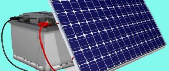
- home
- Green electrics
Solar power plants are not yet widely used, for a number of reasons described in this article (opens in a new window). Thin-film solar cells, among the latest technologies, have not yet become fashionable and are not used everywhere, because... have more disadvantages than advantages, but let's consider both sides.
What is the difference
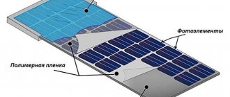
The fundamental difference lies in the materials used. To achieve the distinctive parameters of thin-film solar cells, it is necessary to use semiconductors from copper indium selenide , as well as cadmium telluride . The principle of operation is exactly the same as in polycrystalline and monocrystalline photocells with the difference that these semiconductors can be applied to film. The film bends and curls, unlike classic solar panels.
Photocells based on thin films of semiconductors
The working element of these cells is thin films of semiconductors, both inorganic and organic.
Photocells based on amorphous silicon
Amorphous silicon thin films are most commonly produced by plasma-assisted vapor deposition (PECVD).
Silane or its derivatives are used as a source of silicon. The deposition temperature is 250-400°C, which makes it possible to use not only metal tapes, but also glass and even polymer films as substrates. In the case of flexible substrates, such as metal or polymer tapes, deposition can be carried out in a continuous process by drawing the substrate tape through the reactor. This technology is characterized by high productivity, and the films are correspondingly low in cost. Amorphous silicon always contains hydrogen in an amount from 5 to 20 at. %, which blocks the dangling bonds of silicon, so it is a hydrogenated form of silicon. Hydrogenated amorphous silicon (aSi:H) is a direct-gap semiconductor with a band gap of 1.7 eV and a high optical absorption coefficient (?>105 cm-1 for photons with energy E>1.7 eV). This means that a film just a few microns thick will absorb most of the solar radiation. When an amorphous silicon film is doped with germanium, the band gap decreases, and when carbon is added, it increases. This makes it possible to create solar cells with two or three heterojunctions, covering almost the entire solar spectrum. The efficiency of photoconversion of such elements reaches 12%. The disadvantage is the degradation of the physical properties of the element under the influence of solar radiation - the Staebler-Wronski effect. To increase the stability of the properties of solar cells, not amorphous silicon is used as a semiconductor, but a two-phase material containing inclusions of micro or nano crystals of silicon in an amorphous matrix, which is known as microcrystalline or nanocrystalline silicon. This material is produced by adding hydrogen to the reaction mixture. At a high content of the crystalline phase, the properties of the material increasingly correspond to the properties of multicrystalline silicon. In addition to cells based on a two-phase material, hybrid cells are being developed: amorphous Si/microcrystalline (nanocrystalline) Si, which are called “micromorphic” devices in the literature. These devices have higher efficiency and stability than devices based only on amorphous silicon. It should be noted that amorphous silicon films have also found another application - as a passivating coating for monocrystalline silicon wafers in first-generation modules. This coating reduces the surface recombination of charge carriers by two orders of magnitude, which leads to a significant increase in photoconversion efficiency. These elements were developed by Sanyo (Japan) and are called “heterojunction with Intrinsic Thin layer - HIT”. Sanyo has launched industrial production of modules based on the HIT structure with a conversion efficiency of 21.5%.
Photocells based on crystalline silicon films
An alternative material to both monocrystalline and amorphous silicon is polycrystalline silicon films.
Polycrystalline Si is resistant to solar radiation similar to monocrystalline material and at the same time provides higher photoconversion efficiency than amorphous silicon. Due to the high electrical conductivity of silicon, solar cells based on polycrystalline material do not require the use of a transparent electrode. However, in such elements it is necessary to use a light-absorbing layer, since the optical absorption in polycrystalline silicon is much lower than in amorphous silicon. The electrical properties of polycrystalline silicon, in particular the lifetime of charge carriers, which determine the efficiency of photoconversion, depend on the size and orientation of the crystallites. Currently, several methods have been developed for the production of polycrystalline silicon films, for example, chemical vapor deposition using hot filament (hot-wire CVD), or the gas transport method using iodine. Both methods have a high deposition rate - up to 3 µm/min, but the second method has some advantages: it works at atmospheric pressure and allows one to obtain coarse-crystalline films with a crystallite size of 5-20 µm. Another method for producing polycrystalline silicon films is metal-induced crystallization of an amorphous silicon film. Unlike the first two methods, when polycrystalline films are obtained directly during the deposition process, in this method the amorphous film crystallizes as a result of its contact with the metal, which accelerates crystallization. Typically the process is carried out at temperatures of 450-600°C and time from 10 to 70 hours. (The average speed of propagation of the crystallization front is 2-3 μm/h at 550°C.) It turns out that the rate of crystallization can be increased if the process is carried out in a constant electric field of moderate intensity. For example, at a field strength of 80 V/cm, the crystallization time at 500°C is only 10 minutes. The effect of inducing crystallization of amorphous silicon is inherent in many metals. These metals are conventionally divided into two groups: those that form a eutectic with silicon (for example: Al, Au, Ag) and those that form silicides (for example: Ni, Pd). The most intensively studied crystallization initiators are Al and Ni, since they are widely used in semiconductor device technology. Despite the fact that the effect of inducing crystallization has been known for about 40 years, its mechanism remains largely unclear. The induced crystallization method makes it possible to obtain high-quality silicon films consisting of large crystallites up to 100 μm in diameter, and in some cases textured silicon films are obtained.
In addition to this method, special methods are currently being developed that make it possible to obtain textured films of silicon and germanium: deposition on an inclined substrate (Inclined Surface Deposition - ISD), deposition in the presence of a high-energy ion beam directed at a certain angle to the substrate (Ion Beam Assisted Deposition - IBAD), deposition onto a metal substrate with a biaxial texture. The first two methods are universal and allow the formation of textured films of various materials on almost any substrate, including polycrystalline and amorphous. The disadvantages of these methods are their high energy consumption and the need to use high vacuum, which makes industrial scaling of these technologies difficult. The third method is already widely used to form textured YBa2Cu3Ox films. Highly oriented germanium films have also been prepared on biaxially textured metal tapes. This made it possible to create a solar module based on thin films of group III-V compounds with an efficiency of 30%. Using this technology, industrial production of solar modules was organized in the USA in 2008 (Wakonda company).
Photocells based on crystalline CdTe films
Cadmium telluride is one of the promising materials for the production of highly efficient and cheap solar modules.
This material is a direct-gap semiconductor with high optical absorption coefficient (~105 cm-1) in the visible range and has a nearly ideal bandgap (1.5 eV) for single-junction cells. Thanks to this, a CdTe film just a few microns thick absorbs ~90% of solar radiation. Currently, a variety of industrially effective technologies for producing CdTe films have been developed, such as sublimation, aerosol deposition or “wet” printing, solution growth, electrodeposition, and various physical evaporation/deposition methods. All these methods make it possible to obtain large-area CdTe films with a high deposition rate: ~1 m2/min. The record efficiency of a CdTe-based cell is 16.5% (see Fig. 1), a commercial size module is 11%; and typical commercial modules have an efficiency of 7–9%. A CdTe-based cell consists of a glass substrate coated with a layer of transparent conductor (SnO2:F, In2O3 or Zn2SnO4), then n-CdS (<100 nm), then p-CdTe (1-3 µm), on top of which a metal electrode is applied ( Ni-Al). The properties of these cells do not greatly depend on variations in the technological parameters of film production, which is convenient for industrial production. Critical aspects of the technology are the recrystallization of CdTe films using CdCl2 as a flux, as well as the prevention of diffusion of Ni into the CdTe film when forming a metal electrode (for this, a small amount of copper is introduced into the electrode composition).
The main disadvantages of these solar cells are environmental and medical problems associated with the harmful effects of cadmium. However, studies have shown that all the requirements for the safe production and disposal of these solar cells can be met at quite reasonable costs.
Photocells based on crystalline films of CuInSe2 (CIS)
CuInSe2 is another promising material for solar cells. The current efficiency record for laboratory devices based on Ga-doped CIS is 19.5%, which exceeds the efficiency of polycrystalline silicon cells. Commercial size modules have an efficiency of over 13%. A typical CIS cell structure consists of a substrate (soda-lime glass, or flexible stainless steel or polyimide substrate) on which Mo (1 µm; deposited at room temperature) is deposited, followed by a layer of Cu(In-Ga)Se2 (~1 µm), then CdS (~70 nm), on top of which a transparent conductive ZnO film (~350 nm) is deposited. Cells with 18.6% efficiency, cadmium-free, were also manufactured in which CdS was replaced by ZnS. To obtain high-quality coarse-crystalline CIGS films, the stoichiometry of copper and indium is varied at different stages of their synthesis. One of the key aspects of the technology is the presence of sodium, for which Na-containing glass is used or sodium is added additionally in the form of various salts in the case of using metal or polymer substrates. The disadvantage of these devices is the difficulty in obtaining high-quality CIGS films due to the complexity of the phase diagram of this quaternary compound, as well as degradation of properties as a result of atmospheric influences. To increase the reliability and service life of photocells based on CIGS films, it is necessary to understand the mechanisms of degradation of their properties and develop an effective technology for their sealing for long-term use in atmospheric conditions.
Photocells based on crystalline films of groups III-V
Semiconductor materials based on compounds of groups III (Al, Ga, In) and V (N, P As, Sb) have been known since 1950, and in the early 1960s the first solar cells based on gallium arsenide were created, which were immediately found Application in space research due to resistance to cosmic radiation and high photoconversion efficiency. Of all the Group III-V compounds, InP and GaAs are the most widely used because they have an almost ideal band gap of 1.4 eV. The highest efficiency on single-junction structures was achieved on thin-film devices formed by vapor-phase epitaxy: 25.8% for GaAs and 21.9% for InP.
A disadvantage of devices based on films of group III-V compounds is the high cost of substrates that ensure epitaxial growth of these materials. In addition, the efficiency of photoconversion of films is very sensitive to impurities and structural defects, which does not allow simplifying the technology of their deposition and reducing the cost of cell production. The solution to this situation is to use cells with several junctions that provide more complete absorption of the solar spectrum, and also to use the concentration of solar energy from a large area onto a small photocell. In this case, instead of an expensive photocell, a significantly cheaper concentrating device is used, for example, a Fresnel lens. As a result, the cost of the photocell decreases in proportion to the degree of concentration of solar radiation. The current record for photoconversion efficiency, achieved on a structure with three transitions at a concentration of 364 times, is 41.6% (see Fig. 1). An increase in the number of heterojunctions beyond 3 leads to a significant increase in the cost of a photocell, so the main market for highly efficient devices with four or more heterojunctions is the aerospace industry.
Rice. 1. Progress in the efficiency of solar cells of various types [1]
Photocells based on organic materials
Recently, solar cells based on organic materials have attracted increasing interest from both researchers and solar cell manufacturing companies. This is due to the constant increase in the efficiency of these devices. Thus, in December 2009, the Solarmer company (USA) reported a photoefficiency of 7.9%, and already in July 2010, the same company announced a new record of 8.13%. Despite the fact that the photoconversion efficiency of organic solar cells looks rather modest compared to inorganic solar cells, these devices have a number of positive properties, thanks to which they are real competitors to inorganic elements. These properties include low consumption and low cost of materials, their environmental safety and cheap disposal, very low production costs, flexibility of modules and the associated ease of transportation and installation. As a result, Solarmer said it will soon achieve an organic energy cost of $0.12-$0.15/kWh, or <$1/W, in line with the best second-generation inorganic thin-film solar cells (see Fig. 2).
Organic semiconductors can be either monomers, such as dyes, or polymers. Doping of organic semiconductors can be accomplished by introducing foreign atoms or molecules. For example, p-type semiconductors are obtained by introducing halogens, a nitro group, organic molecules such as 2,4,7-tyrnitrofluorenone or ortho-chloranyl, as well as semiconductors with high electron affinity: fullerene or pyrylene diamide. n-type conductivity can be obtained by introducing alkali metals or semiconductors with low ionization potential.
The simplest architecture for a polymer photocell is a planar heterostructure, in which an electron acceptor film is applied to a photoactive polymer film (donor), and electrodes are applied on both sides. Currently, polymers with conjugated C-C bonds modified with fullerenes are used as photoactive materials. In polymer semiconductors, unlike inorganic semiconductors, an absorbed photon generates an exciton, i.e. electron-hole pair bound by Coulomb forces. This electrically neutral quasiparticle diffuses to the donor-acceptor interface, where it dissociates into free electrons and holes, which contribute to the photocurrent. The typical diffusion length of excitons in organic semiconductors is 1-10 nm. The photoactive polymer film should be the same thickness, but at this thickness this film has a very low optical absorption coefficient. One of the ways to solve this paradigm is the use of bulk heterojunctions, when the donor and acceptor materials form a phase-separated system, for example, during the stratification of a polymer solution or during the depolymerization of a block copolymer solution with subsequent polymerization of two phases from the constituent monomer blocks, for example, during the ordering of a block copolymer solution . By varying materials, solvents, their concentrations and process conditions, it is possible to obtain interpenetrating systems of phases with a characteristic size of 1-10 nm. Another solution is to create ordered heterostructures. Most often this concept is implemented in so-called hybrid, i.e. organic/inorganic structures, for example, when a photoactive polymer fills the pores of TiO2, or silicon nanoparticles fill a polymer matrix, forming a percolation system, or a structure of InP nanorods grown on a conductive substrate is filled with a polymer.
The disadvantage of photocells based on organic materials, in addition to the low efficiency of photoconversion, is the problem of stability of properties inherent in conjugated polymers.
Rice. 2. The cost of solar electricity as a function of the efficiency and price of various PV modules. [2] The three highlighted areas represent three generations of solar cells. The blue line, o (Balance Of System costs), indicates the minimum limit of costs associated with installation and maintenance of installations, land costs, etc. For modern modules based on monocrystalline silicon, these costs are approximately 250 US$/m2 .
Dye photocells
Dye solar cells also belong to thin film solar cells. This type of solar cell was invented in 1991 by the Swiss scientist Gratzel, and is therefore also called the “Gretzel cell”. The first Gretzel cell consisted of an anode (10 µm thick) of highly porous nanocrystalline titanium dioxide, the surface of which was coated with a monomolecular dye layer and which was formed on a glass substrate coated with a layer of transparent conductive oxide. The porous anode was impregnated with liquid iodine electrolyte. The cathode was platinum.
The Gretzel cell works as follows. Light passing through a transparent substrate is absorbed by a photoactive dye. Electrons excited by light in the dye pass into TiO2 and diffuse to the transparent conducting electrode under the influence of their concentration gradient. The electrolyte completes the electrical circuit and transports electrons from the cathode (Pt) to the dye, where they recombine with holes left by migrated photoelectrons. Thus, in a Gretzel cell, the semiconductor (TiO2) is used only to transport photoelectrons, which are generated in the photosensitive dye. In this way, the Gretzel cell fundamentally differs from conventional semiconductor photocells, in which both the transport and generation of photoelectrons occur within the bulk of the semiconductor.
The disadvantages of the Gretzel cell are the high corrosivity of the electrolyte and the high cost of platinum. However, these problems are not fatal and effective solutions can be found for them. For example, it has already been proposed to use CoS instead of Pt, and less aggressive organic electrolytes have also been proposed.
Currently, the record photoconversion efficiency of dye cells is 11.1%, which, given the low cost of the materials used and the simplicity of the technology, makes these photocells attractive for mass use.
Research is constantly being conducted to find new cheaper and/or more efficient materials, which allows us to hope for increasing the efficiency of these structures. In addition to this usual “evolutionary” path, the efficiency of photoconversion can be significantly increased if tandem structures are used. A standard Gretzel cell operates as a photoanode when photocurrent arises from the photogeneration of electrons in a photoactive dye. Similarly, a photocathode can be created when the photoactive dye generates holes, or in other words, the photoexcited dye induces electron transfer from the p-type semiconductor to the dye. If two such structures, working as a photoanode and a photocathode, are combined into one element, the photoconversion efficiency can be significantly increased. Work in this direction is underway, but so far the efficiency of such tandem structures is lower than that of a standard n-type Gretzel cell, since existing p-type cells have a small photocurrent, which is a limiting factor for the entire structure.
____________________
- [1] https://en.wikipedia.org/wiki/Thin_film_solar_cell
- [2] NS Lewis. Toward Cost-Effective Solar Energy Use. Science 315 (2007) 798-801.
Source: https://www.superox.ru/photoelements2.htm
Related posts:
- Comparison of thin film and...
- Solar market prospects...
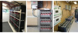
- Prosolar-R batteries
- Questions and answers on…
- Solar controller Prosolar SunStar…
- Your own network
- How to choose an uninterruptible unit...
- Autonomous power supply
Advantages
- Translucency. Classic (polycrystalline and monocrystalline) solar panels are completely opaque. Amorphous thin-film batteries can be designed to replace a window in a home, letting in some light and converting some into electricity.
- Ease. Batteries made on film are several times lighter than classic ones, which gives more freedom in installation and simplifies operations with them.
- Flexibility. Thin-film batteries theoretically be bent in any plane without loss of performance.
- Impact resistance. The film does not break from falling during installation or from hail and remains operational in the most extreme conditions.
Flaws
- Low efficiency. If we do not consider laboratory samples, but evaluate the real performance of manufactured models, then at the output we will obtain an efficiency of no higher than 4%, which is three times less than that of a polycrystalline photocell.
Important. When using translucent photocells, the coefficient drops to a ridiculous 2% and you can hardly even charge your smartphone from one window. - High price. When compared with classic solar panels, their price per sq.m. comparable to the same polycrystalline models, but the power will be three times lower. If we compare panels of the same power, the picture will look like this (data from Aliexpress.com):
Comparison of film and silicon solar panel pricesThe difference in price is exactly three times, with the same power
- Reduced performance when heated. If in poly/monocrystalline batteries this figure reaches 12% of the rated power, then in flexible solar cells it reaches 30-40%.
Disadvantages of thin film amorphous silicon panels
- Amorphous thin-film solar cells have lower efficiency than mono- and polycrystalline solar cells. Attempts to increase it, for example, by creating multilayer modules or doping with germanium to reduce the bandgap and further improve light absorption, are quite complex processes that make production more expensive. If these processes are implemented, thin-film panels will cost more and therefore lose their competitive advantage.
- Thin film modules tend to degrade faster than mono- and polycrystalline solar panels. The expected lifespan of amorphous batteries is shorter than that of crystalline batteries. It is not always possible to determine how much, especially given the constant development of technologies used in the production of thin-film panels. Today, the service life of such panels, on average, ranges from 10 to 25 years, and they lose about 10 to 40% in power in the first few seasons, after which their power is fixed at this indicator and, as a rule, does not fall. . Many manufacturers promise a power output of about 80% by the end of their service life.
- Large footprint. You need to cover a much larger surface area (about 2.5 to 3 times) with amorphous silicon solar panels than with crystalline panels to get equal power.
Solar panels made of amorphous silicon are constantly being improved and today have encouraging prospects. They are lighter in weight, more flexible and potentially cheaper to produce. On the other hand, this technology must become more mature to compete with mono- and polycrystalline solar cells.
Myths and reality
So far, the manufacturing technology of film solar cells is not a real competitor to poly/monocrystalline analogues. Primarily due to the high cost of the materials used. However, there are several myths circulating on TV, online and among retailers about the miraculous properties of this technology.
- Thin film solar panels can operate in cloudy weather. This is partly true, but it is also true that any solar panels work in cloudy weather , while delivering less current or voltage, depending on the model. Film ones also definitely reduce their productivity.
- Film batteries do not reduce performance when heated. This is an outright lie. The performance degradation is much greater than the poly/monocrystalline counterparts. Therefore, when installing such panels, it is imperative to provide for the possibility of ventilation of their rear walls.
- Cheaper. Actually more expensive (see disadvantage 2)
- Can take any form. There is truth here, but as practice shows, this is of no use. The panels are arranged in a plane to achieve maximum effect.
- You can roll them into a tube and then the light will shine on them almost all day. Indeed, such a “sensational” invention brings an increase in performance that is less than using the same area of similar batteries in a flat form.
Scheme of operation of a cylindrical module - Extended service life. Not really. The service life of a film panel is 10-12 years, while polycrystalline models last from 15 to 20 years.
- Can be used instead of glass in windows. At the same time, you will practically not see the streets, and the efficiency of such a translucent panel will allow you to charge one mobile phone from one window throughout the day. A dubious advantage.
- Environmentally friendly. Because While batteries use semiconductor alloys of indium and cadmium, much less silicon is used. At the same time, sellers claim that silicon is a substance in terms of harmfulness between uranium and arsenic, forgetting that 1/3 of the earth’s crust consists of it.
- Payback time. Advertising for film batteries says that they pay for themselves within 2-3 years of operation. Not really. The service life of film solar panels (10-12 years) and their cost do not allow them to pay off at all at current electricity prices.
From flat to cylindrical
Cylindrical solar panels were first developed by a small American company with the catchy name Solyndra (from the words “solar” and “cylinder”). They presented their achievement in 2008 and immediately received several large orders from European and American companies. According to them, this figure was more than $1 billion.
Until 2008, solar cells were flat in shape. Solyndra proposed installing cylinder elements in solar panels. A thin layer of photocell is applied to the surface of a glass tube, after which it is placed in another similar tube, but with electrical contacts. The already familiar copper, gallium, selenium and indium are used as semiconductors for elements. Cylindrical solar panels, due to their shape, absorb more light and, as a result, have a higher performance indicator. Each panel consists of 40 cylinders and measures 1 by 2 meters.
To increase the absorbed light, it is recommended to use cylindrical batteries in combination with a white roof covering. In this case, the rays reflected from the roof will pass through the cylinders, which will provide another plus 20% of the absorbed energy. Another important advantage of batteries with cylindrical elements is their resistance to strong winds. They are able to withstand wind gusts of up to 200 km/h. This makes installation of solar panels easier and cheaper.
Application area
As practice shows, it is advisable to use flexible solar panels only in camping conditions. It is much easier to unroll a canvas with film solar panels on the roof of a tent or trailer than to carry around a rigid structure that takes time to assemble. Portable power stations are also popular for charging phones and flashlights while traveling.
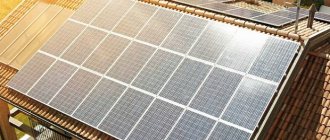
Due to low efficiency, the scope of application of solar panels is very limited. Application as a stationary solar power plant is possible, but only if there is large free space.
Video about film batteries
A typical advertising story, where the announcer tells wonders about film solar batteries, assuming an efficiency of 10%, forgetting that such results have so far been achieved only in laboratory conditions, but not in industrial samples. The video will be of interest to those who want to know how advertising tries to deceive us.
The most interesting achievements in the world of thin-film modules
2 years ago, specialists from the Moscow State University laboratory developed roll-type organic solar cells based on a polymer as an active layer and a flexible organic substrate. Their efficiency was only 4%, but they could operate effectively at a temperature of 80°C for 10 thousand hours. Their activity did not end there; research is ongoing; solar cells based on polymer materials are chosen as the main focus.
Specialists from the Federal Laboratory of Technology and Materials Science in Switzerland have created a solar cell on a polymer substrate with an efficiency of 20.4%. Four elements were used as a semiconductor: selenium, indium, gallium and copper. To date, this is a record figure for solar cells made on the basis of the listed elements. The previous record was 18.7%.
For thin-film solar cells based on indium, selenium and copper, the maximum efficiency value today is 19.7%. The Japanese company Solar Frontier was able to achieve this figure. Absorbing films were applied to photocells by sputtering using heat treatment in selenium vapor.
ICP Solar Technologies has introduced an original folding solar panel. It is enough to roll it out in a sunny place and you can connect the device that needs to be charged. Battery power is 5 W with a supply voltage of 12 V. Agree, an indispensable option for all tourists, although not the only one. Various companies are developing such portable SBs. So, the folding solar battery Foldable Solar Chargers, whose maximum power is 190 W, is no less popular.
Well, the most interesting development can be called “fabric” solar panels. Japanese scientists decided to combine tiny cylindrical solar cells measuring only 1.2 mm and a fabric sheet. This unusual solution will allow us to create high-tech materials for clothing and portable awnings.
The future will tell whether thin-film technology will take the lead in solar cell production. But judging by the active research being carried out in this area and the good results, it is quite possible that in the near future scientists will still be able to create not just efficient solar panels, but also ones that will be accessible to the general population.
This video talks about solar modules based on thin-film technology, which make it possible to convert up to 10% of solar radiation into electricity and at the same time increase the efficiency of photocells by one and a half times, and reduce silicon consumption during production by 200 times!
Comments:
Megavolt
I read that they released solar batteries in the shape of a round cone, they produce 20% more than conventional batteries. Does anyone know about this technology?
Electrician
Megavolt, let's calculate))) The efficiency of film batteries (namely, they are rolled into a cone) = 10%. We add 20% of 10% to them and get as much as 12% with an increase in cost of at least three times! Breakthrough in savings!
Semyon
Electrician, I also watched this story. It immediately seemed suspicious to me that the entire scientific breakthrough consisted of giving batteries some kind of shape. As if no one had guessed before that the sun was out of place... As always - conspiracy theories and collusion.
Leave a comment Cancel reply
Related Posts
Pros and cons of vertical wind generators, their types and features
Do solar panels for a private home pay off?
How to choose a solar panel - overview of important parameters
Windmill for a private home - a toy or a real alternative
Advantages and disadvantages of solar devices.
A significant disadvantage of unique batteries is that their area is 2-2.5 times larger than standard silicon polycrystalline modules. Having not very high efficiency, thin-film solar batteries are not profitable to use in compact systems. Due to this disadvantage, the main application of this type of module is in the field of large lighting installations with a power of more than 10-15 kW.
What makes people use thin-film solar panels at home?
There are several answers to this question:
- availability of this energy source,
- uninterrupted operation, especially in sunny countries,
- autonomy, that is, use anywhere, regardless of the presence of accompanying factors,
- the absolute environmental friendliness of this type of energy production, compared to established sources,
- constantly decreasing cost of sets of such modules, due to constant improvements,
- the inexorably increasing efficiency of batteries helps them compete with standard energy sources,
- absolute accessibility for any person, since the installation of such devices does not require any approval, and in some countries entails additional government subsidies that encourage residents to use environmentally friendly sources.
Many may think that installing solar modules can only be done by wealthy people, but this is far from the case. There is no doubt that the initial stage will require considerable investments in purchasing and equipping a home with such sources of free energy. But, after some time, the savings will begin to show results, and if we take into account the factor of the constant increase in the cost of electricity, the upcoming benefits may exceed all expectations.
Energy savings don't end with appliances. By installing water collectors, which will help save up to 70-80% of electricity on water heating and heating, you can get pretty decent work results. By installing solar panels of sufficient power, you can significantly replenish the family budget with savings in the winter. The fact is that in such cold times, a fairly large amount of energy is spent on heating the home. Using water collectors, any solar panels, even thin-film ones, will bear fruit.
It is worth mentioning the disadvantages of batteries, since this source has plenty of them.
These include:
- many available solar panels have a low level of efficiency,
- any elements of this type require constant monitoring and care so that the productivity of the entire complex does not decrease,
- high temperature reduces power generation, and in the absence of cooling elements in module installation kits, this issue becomes quite relevant,
- the negative impact of time on the power of installations, since over time the crystals cease to produce the initially declared amount of energy,
- high cost of the entire scheme.