Photodiodes are ordinary semiconductor diodes, but they convert light into electricity. These are the same solar batteries, as well as elements that respond to light in a variety of relays, sensors, microcircuits, and especially in fiber optic systems, equipment related to light (UV, IR), its intensity. In these same areas, LEDs, phototransistors, and photoresistors are used, but they and the drawings for them should be distinguished. We will describe what a photodiode is, how it functions, its types, its components, how it is included in assemblies and on device boards, and we will also describe circuits with these radio components.
Photodiode concept
A photodiode, PD, is a semiconductor part, the same diode as it passes current in one direction, with a pn (pin) junction, but from a material that changes its qualities under the influence of optical radiation, initiating processes that create electric current.
If the light is completely absent and does not fall on such a radio component, then in a calm state, in equilibrium, it has qualities similar to a simple diode.
If UV or IR radiation hits a sensitive area, the element begins to react, converting this flow into electricity.
It is necessary to distinguish between different radio components with the prefix “photo”:
- the photodiode we are considering. The essence of a “photo” or “opto”, “galvanic” (such names are used less frequently) diode, which immediately distinguishes it, can be briefly expressed in one sentence: the part converts light into current;
- phototransistors. “Two in one” is a photocell and a transistor combined in one housing, which opens depending on the amount of light supplied. That is, if in the diagrams we discussed below these elements are separated, then in this case they are in the same crimp. Instead of a bunch of individual specified parts, you can use such a one-piece spare part if it fits the parameters;
- photoresistors. They change the resistance (this is the key parameter here) depending on the light level.
As you can see, “photo” radio components can be used for very similar, in some cases similar purposes (for example, sensors, relays), but the circuits will be different, taking into account the differences in the operating principle of each type.
You also need to know the designation of different elements on the diagrams. The photodetector has two arrows directed towards it, and there is logic in such graphics: the product perceives radiation.
The LED often cooperates in circuits with a photodiode. The first initiates the operation of the second: it is placed opposite, and when turned on, a stream of light falls on the first element, activates it, and it sends a signal to the actuator unit. This principle is used for remote controls, various IR signal receivers, as well as for optical (laser) alarms that are activated if the light stream is crossed by an intruder.
So, the photocell converts the light falling on its sensitive segment into an electrical charge. This process occurs due to the occurrence of special processes during the movement of charge transporter particles at the atomic level during irradiation of the pn zone. This phenomenon is caused by changes in the properties of the materials used (semiconductors).
If on photoresistors it is the conductivity that changes when the charge transporters move, then on photodiodes a current appears at the closing segments of the pn junctions - this is their difference.
Structure
A regular LED has the same structure as a “photo”, but the latter has a window so that the light falls on the part that receives it.
Photodiode structure diagram:
Photoconductive and photoelectric modes of operation of photodiodes
In this article we will look at the advantages of two types of photodiode circuit implementations.
When should photoelectric and photoconductive modes be used when installing photodiodes in electrical circuits? In this article we will discuss the details of these modes and project options associated with them.
This is the third part of our Introduction to Photodiodes series, which explores the technical details of these devices, which respond to high-frequency electromagnetic radiation in various forms:
Principles of operation of photodiodes
We will try to describe as clearly as possible, in simple words, the principle of operation, the properties of the photodiode, how it functions, how electric particles move and interact with the pn sections:
- In the figure below there is a semiconductor: on the left is the p-variant, on the right is n. On the first, the number of “holes” (they are also positively charged electrons) is excessive, on the second, there is an excessive number of free electrons.
- Diffusion occurs - holes penetrate into segment n, electrons penetrate into segment p. The remaining particles pass through, forming a barrier layer that prevents the movement of the first and second.
- If voltage is applied: “+” on the left, “−” on the right, then current will flow as the blocking layer will be overcome. When voltage is applied, on the contrary, this layer will become large, the current value will be very small, approaching or equaling zero.
- The photosensitive location of the photocell is n. If this segment is darkened, then its behavior is similar to a conventional diode. When light or electromagnetic waves hit it, electrons are knocked out of the outer layers of the atoms. Their number and holes (together these are photocarriers) increases, the particles diffuse in different directions (towards the contacts of the part - anode, cathode). At the pn junction, holes are transmitted, but electrons are retained. A potential difference, an electric current, appears.
This is what the diode looks like in a quiet state:
More complex explanation:
- The radiation is directed perpendicular to location pn. The energy at which photons are absorbed becomes greater than the band gap, and electron-hole pairs—photocarriers—are formed;
- When phototransporters penetrate into the n-region, most of them (not all) do not have time to break up into components and end up close to the boundary of the pn region, where they are separated by an electric field;
- In the described process, holes end up on the p-segment, but electrons cannot penetrate the field enveloping the transition, so they accumulate near the n-region and at the edge of the transition.
- The particles each move towards their own electrode, thus a current arises; its flow through the junction is completely dependent on the movement of holes; this version of it (in which photocarriers participate) is called drift current or photocurrent.
You can very briefly express how a photodiode generates current as follows. A consequence of the concentration of holes and electrons at p and n locations, respectively, is the formation of a potential difference. The same phenomenon is an electromotive force that creates a reverse current, cathode⇒anode, and in the external circuit it will be the other way around. This is a solar (helio) electric panel (battery).
Photodiode modes
Applications and types of photodiode have their own nuances depending on the mode for which it is used.
There are two main modes based on the method of using the process of converting radiation into current:
- photovoltaic (generator) - these are the same solar panels. Small ones are used for calculators, stand-alone lamps and the like. Large ones - for autonomous systems for providing electricity to houses, cars and other things. These are power sources;
- photodiode (converter). With external reverse voltage. For controlling various devices. For example, for lighting with automatic shutdown after sunrise. In the absence of radiation, the element is an ordinary diode, it passes current, but during the day it blocks the flow.
In converter mode, the part acts as a light-controlled switch, for which it is connected to the circuit in forward bias - with the cathode to “+” and the anode to “−”. In the dark there is only reverse, dark current (Irev, units and tens of μA). In light, a photocurrent is added to this, depending only on the intensity of the radiation (tens of μA); the stronger the radiation, the more powerful it is.
The photocurrent is calculated by the formula: Iф=Sint×Ф. Where the first component is the integral sensitivity, the second is the luminous flux.
How do the two photodiode modes differ?
In converter mode, the diode is biased in the reverse direction by voltage. The photocurrent that appears under illumination is at the same time a function of the power of the luminous flux. With a generator, the part creates a photoEMF. In other words, when radiation hits the pn junction, a voltage proportional to the flux intensity appears at the output of the element.
The photodiode (converter) operating algorithm is more often used for prompt powering of devices. Its advantages: higher performance, greater sensitivity to optical radiation, wider dynamic range. But there is a significant disadvantage - there is a noise current flowing through the load. Sound effects are reduced by cooling the part to −10° C, but this is expensive. Sometimes because of this, when there is a need for absence of noise, preference is given to the galvanic (photovoltaic) operating algorithm
When using the conversion algorithm, the power source is connected with reverse polarity, here the purpose of the photodetector is to act as a light sensor.
The principle of operation of a photodiode, the circuit and structure of a photodiode
What is a photodiode? It is a semiconductor that creates an electric current when exposed to light.
Photodiode operation diagram
To understand the working of a photodiode, let's first understand the working of a diode. A diode is a semiconductor that allows current to pass in one direction.
Diode at rest
On the left in the figure is a p-type semiconductor, on the right is an n-type, in other words, on the left is an excess of “holes” (positively charged atoms), on the right is an excess of free electrons. As a result of diffusion, holes enter the n-region, and electrons enter the p-region. At the boundary of the regions, some holes and electrons recombine. The rest pass through, creating a barrier layer that prevents the movement of holes and electrons.
If you apply voltage: on the left - plus, on the right - minus, current will flow, since the blocking layer will be overcome. If the voltage is applied in reverse, the blocking layer will increase and the current will be zero or very small.
The photodiode has a photosensitive n-region. If it is darkened, it behaves like a regular diode. Light - electromagnetic waves - entering the n-region of the photodiode knocks out electrons from the outer shells of atoms. Many holes and electrons (photocarriers) appear, which diffuse in all directions. A pn junction allows holes to pass through but retains electrons. Electric current occurs.
Characteristics of photodiodes for selection
Photodiode parameters can be found in their specifications online. Let's look at the items by which parts are selected. It should be said that for simple purposes (light relay, IR receiver), the characteristics listed below can be ignored; it is enough to buy the recommended product for a specific assembly.
Current-voltage qualities that determine changes in luminous flux values according to changing voltage with a stable radiation flux and dark current. Below is a standard I-V diagram of a photodiode.
Spectral qualities (sensitivity). They display how the wavelength of light and the angle of incidence of the rays change the characteristics of the photocurrent on different semiconductors.
Sensitivity can be measured under different light parameters:
Light or energy characteristic. Explained in the picture below:
Temporary constant. The period during which the current responds to an increase/decrease in dimming or illumination by 63% of the set value.
Lower limit of sensitivity. Minimum light intensity for a photodiode reaction to occur.
Dark resistance. Characterizes the state of the semiconductor in the absence of light; this is the current-voltage characteristic in the absence of radiation.
Inertia:
The above main characteristics are used to select photodiodes for load parameters:
Definition of optocoupler (optocoupler)
An optocoupler is a semiconductor device containing a radiation source and a radiation receiver, combined in one housing and interconnected optically, electrically, or simultaneously by both connections. Optocouplers are very widespread, in which a photoresistor, photodiode, phototransistor and photothyristor are used as a radiation receiver.
In resistor optocouplers, the output resistance can change by a factor of 107 ... 108 when changing the input circuit mode. In addition, the current-voltage characteristic of the photoresistor is highly linear and symmetrical, which determines the wide applicability of resistor optocouplers in analog devices. The disadvantage of resistor optocouplers is their low speed - 0.01 ... 1 s.
Vasiliev Dmitry Petrovich
Professor of Electrical Engineering, St. Petersburg State Polytechnic University
Ask a Question
In circuits for transmitting digital information signals, mainly diode and transistor optocouplers are used, and for optical switching of high-voltage, high-current circuits, thyristor optocouplers are used. The performance of thyristor and transistor optocouplers is characterized by switching time, which often lies in the range of 5...50 μs. For some optocouplers this time is shorter.
Let's take a closer look at the LED-photodiode optocoupler. Let's give a conventional graphic designation for this optocoupler (Fig. 1.131, a).
Recall that the emitting diode (on the left) must be turned on in the forward direction, and the photodiode must be turned on in the forward direction (photogenerator mode) or in the reverse direction (photoconverter mode).
Let's use the generally accepted choice of conditionally positive directions for the currents and voltages of the optocoupler diodes (Fig. 1.131.6).
Let us depict the dependence of the current iout on the current iinx at uout = 0 for the optocoupler AOD107A (Fig. 1.132).
The specified optocoupler is designed to operate in both photogenerator and photoconverter modes.
Options, types of photodetectors
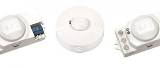
The infrared photodiode is made in a black housing and reacts only to IR radiation. The dark color of the lens is a kind of filter tint so as not to interfere with other spectrums.
Photodetectors have a frequency range, here it is orders of magnitude larger, up to 10 MHz (much higher than that of photoresistors), which ensures excellent performance. For pin variants and with a Schottky barrier this figure is 100 MHz–1 GHz, for avalanche variants it is 1–10 GHz.
We will consider the types of photodiodes based on their operating principle, combination options, placement of layers, and materials below.
Photodiode pin
Pin-type elements are widely used for fiber-optic communication systems - they convert light into electrical signals, which are then converted into information (video, sound, etc.)
The p and n layers are made using doping: impurities that enhance it are added to the semiconductor material. If there is a + in the designation of such a part, then this indicates an increased content of additives.
The middle segment - part "i" - is the conductor "n", but lightly alloyed. If a reverse voltage is applied to it, then a depleted location is formed there (there are fewer holes/electrons).
The resistance on the i-segment increases, much higher than that on p+ and n+. The result of this process: the electric field is concentrated in the i-region, the photon absorbed there creates a pair: electron/hole. A powerful field in the i-section instantly distributes them to the electrodes: the hole is absorbed by the cathode, the electron by the anode. This creates an electric current.
The efficiency of pin photodiodes is extremely high, since their frequency can reach 1010 Hz, which guarantees the transfer of terabytes of data in 1 second. For such parts, the i-section is much wider than the p+ and n+ so that photons are absorbed more precisely in this segment.
Avalanche
In fiber optic technologies, in addition to the pin types of the parts under consideration, special types are used - avalanche photodetectors (APDs), their difference is an additional p-section.
Due to the reinforcing additives, the p-layer has a higher resistance and, accordingly, the greatest decrease in voltage across it. The photon, finding itself in the light-sensitive i-segment, pulls out an electron from there, rushing to the anode, the hole goes to the cathode.
On its route, the electron ends up at a location of high voltage in the p-layer, here it accelerates sharply, which allows it to knock other similar particles out of the shells of the atoms of the p-section. Then the newly formed free electrons do the same - they knock out additional analogues from the valence segments. The phenomenon is growing like an avalanche.
The image visualizes a sharp surge in the driving electric force on the p-layer. The primary current that appears in the i-layer grows like an avalanche in the p-section. The increase reaches several hundred times, but if it is too large, it creates noise that increases faster than the pulse. The optimal coefficient value is 30–100.
With Schottky barrier
In this type of element, several films are created, that is, a special structure that allows one to avoid the injection of minority carriers. Such parts use the movement of only the main transporters. The advantage is that there are no slow processes influenced by the phenomena of accumulation and resorption of secondary carriers based on the diode. Pros: inertia, recharging times are negligible, the first is determined only by the time of passage of carriers through the space charge regions.
The above abilities allow the use of optodiodes for microwave modulation of radiation.
Heterostructural
They are assembled from 2 semiconductors with different sizes of the forbidden segment; the section between them is called heterogeneous. A special selection of materials is used to create a device that covers (perceives) the full extent of the waves. The disadvantage of such a product is the cost of production.
Checking the photodiode with a multimeter
Let's look at how to check photo detectors with a multimeter. The tester measures the resistance values (reverse and forward) during the process of lighting/darkening the diode. The multimeter (or ohmmeter) is set to 200 kOhm.
Sometimes a characteristic defect occurs - a chaotic change in current (“creep”). To detect a problem, assemble a simple circuit (see figure below) and measure the amount of reverse current for several minutes. If the current is constant, then the part is working. You can check the spare part on the board, but errors are possible, so desoldering is always recommended.
Circuits with photodiodes, where examples of assemblies are used
Photodiodes are used:
- for a fairly narrow specific area - for fiber-optic data transmission systems (FOSS, FOCL). Even electronics engineers do not encounter this area very often. This is where the characteristics we briefly discussed (volt-voltage characteristics, sensitivity, etc.) are especially relevant for calculating photodiode structures.
- solar panels. Such products are connected according to the usual circuits according to the instructions for this product;
- optocouplers, optocouplers that respond to alarm light, various relays, automation, sensors, as well as IR radiation receivers (remote controls, similar control devices).
Photodiode Circuit Basics
The switching circuit for each of the two modes is different. Below is a typical drawing of connecting the device as a converter. Please note: connected in the opposite direction relative to the power source.
Like a generator. When light enters, voltage appears at the terminals, short circuit currents in this mode are equal to tens of amperes, which is reminiscent of the operation of solar batteries, but here the power is small.
An important note about relay circuits: the trimmer is needed to adjust the sensitivity, and without a resistor in the collector line, the optocoupler may burn out.
Circuit diagram of a simple photodiode relay
Build with 320 photo detector (very popular specification). Like other such parts, it can be tested with a multimeter to find out where the anode/cathode is. In this case, the tester values differ if the diode is dimmed.
If a photodiode works as a sensor, relay, or remote control element, and this is the majority of household appliances, then it is turned on in the opposite direction: the cathode to “+”, the anode to “−”. (“photoresistor” connection). In shading, reverse resistance. element is very high, with more radiation it decreases. This feature is used to control equipment.
In Fig. above is a simple relay:
- VD1 is a photodiode and to it R1 is a variable. Resistance the first decreases with decreasing light intensity;
- VT1 is a transistor. The voltage at its base increases if you illuminate it, and it opens at a certain point in the period of light supply, the same will happen with VT2;
- After the above processes, current will flow to the winding of release K1 - the node will switch. If you place the part in the shade, the voltage on VT1 will drop, the transistors will lock, the contacts will open, and the relay will be deactivated.
R1 is a trimmer; it adjusts the sensitivity of the photo relay so that it is activated only from a flashlight. Such a relay can be used as a simple remote control system, and the backlight will work as a remote control.
The components of the circuit are simple and accessible:
- photocell 320. You can also take other models: 263. Before installation, check where the anode/cathode is. Use a multimeter, a procedure similar to that for simple diodes. It’s also a good idea to check the diode’s reaction to light;
- transistors KT3102 and 814;
- e/m relay WJ118-1С. You can take something else, but it is recommended that the winding be from 200 Ohm and for 10 - 15V.
How to work with the scheme. After assembly, move the R1 variable knob to set the max. resistance Place the board away from direct light. When assembling, be careful not to reverse the polarity. Connect the power (you must also follow the previous recommendation). There should be no operation or click on the relay. If this happens, turn selector R1 to turn it off. Now, you can experiment with a flashlight: illuminate it and observe how the relay turns on.
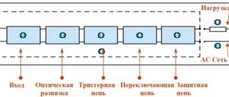
Remote switch circuit
Above is a switch controlled by a small flashlight, a laser. 2 photodiodes used: for on. you need to direct it to VD2, to turn it off. - on VD1. The sensitivity is adjusted by variables R1 and 2. An RS trigger was installed on the D1 chip (K561LA7) for on/off. relay.
When VD2 is illuminated, its resistance. decreases, and the voltage at the input. D1.2 will increase to the level of logical one. On vacation D1.2 will appear 0, the trigger on D1.3 - D1.4 will go to the state when the output. D1.4 will be a logical one. It will also unlock VT1, current will flow to the relay. In the absence of light, the trigger remains and the release will be activated.
All working similar photo relay assemblies have a similar algorithm. To turn it off, you need to light VD1: the reaction of the trigger to output will change. D1.3 will be 0. The VT1 key will be disabled, the relay will be deactivated and will remain so when the light disappears. So: to trigger it you need to shine the light on VD2, to turn it off. - on VD1. The gap between the diodes is 5 cm, which is enough for control with a laser pointer.
The adjustment consists only of setting the sensitivity of the photocells using adjusters R1 and 2. Such a switch must be placed so that there are no significant differences in radiation intensity or direct rays on the lenses. Flashlights operate from 2–3 m. For laser pointers at night, at a setting of max. sensitivity - 20–30 m, during the day this figure will be lower, since less sensitivity is set
In the example under consideration, the relays and diodes are similar to those in the drawing from the previous section. Microcontrollers: K561LA7 or 1561LA7, 176LA7. The KT815 conclusions are located like those of the KT814.
More photo relay drawings
Assembly and connection drawing of a photo relay for street lighting, the device is triggered in the absence of light:
In the assembly below, you can use a photodiode instead of a photoresistor:
A simple photo relay to turn on the light when it gets dark:
Robot running away from the light
A robot from a computer mouse body, leaving for shaded locations:
The robot is controlled by a flashlight:
Electronic mousetrap using photodiodes
Elements:
- any IR photodiode;
- electromagnet. You can take it from used household appliances or make a coil yourself (there are plenty of instructions on the Internet);
- KT 3107 (transistor) provides sensitivity to the galvanic diode;
- We install KT818 because the electromagnet is a fairly powerful load (for our situation, half an ampere is a lot);
- resistor. Without it, the circuit will react even to simple light.
Manufacturing process: we assemble the housing, diodes (photo and light) opposite each other, further from the entrance (when the light flow crosses, there will be a trigger) so that the mouse can pass between them. Above the entrance is a magnet with a lattice door. The circuit also has a power source - a 9 V crown. The standard principle is used: an LED supplies radiation to a photodiode, which perceives light and gives a signal to an electromagnet that closes the mousetrap input.
Circuits with photodiodes on Arduino
There are also many assemblies of various relays and IR receivers based on the Arduino microcontroller.
IR Receiver:
Simple control panels: