Field effect transistor - what is it
It includes three main elements - source, gate and drain. To create them, n-type and p-type semiconductors are used. They can be combined in one of the following ways:
- The drain and source are n-type and the gate are p-type. They are called npn type transistors.
- Those that use pnp polarity. The type of conductivity of each part of the transistor has been changed to the opposite in comparison with the previous version.
Checking with a multimeter
If this part is connected to a power source, then there will be no current. But everything will be different if this is done between the source and the gate or the drain and the gate. It is necessary that a voltage be applied to the gate corresponding in sign to its conductivity type (positive for p-type, negative for n-type). Then current will flow through this part. The higher the voltage applied to the gate, the stronger it will be.
The difference between a field-effect transistor and a bipolar transistor
The transistor will become open provided that a potential difference of the required polarity is applied to the gate. In this case, with the help of an electric field, a channel is created between the source and drain, through which electric charges can move. Other types of transistors control based on current rather than voltage.
The electronic components in question are also called mosfets. This word comes from the abbreviation MOSFET - Metal Oxide Semiconductor Field Effect Transistor (translated this means: metal-oxide-semiconductor field-effect transistor).
Varieties of field beetles
Where to begin?
Before checking any element with a multimeter for serviceability, be it a transistor, thyristor, capacitor or resistor, it is necessary to determine its type and characteristics. This can be done by marking. Once you know it, it won’t be difficult to find a technical description (datasheet) on thematic sites. With its help, we will find out the type, pinout, main characteristics and other useful information, including replacement analogues.
For example, the scanning on the TV stopped working. Suspicion is raised by the line transistor marked D2499 (by the way, a fairly common case). Having found a specification on the Internet (a fragment of it is shown in Figure 2), we receive all the information necessary for testing.
Figure 2. Specification fragment for 2SD2499
There is a high probability that the datasheet found will be in English, no problem, the technical text is easy to understand even without knowledge of the language.
Having determined the type and pinout, we solder the part and begin testing. Below are the instructions with which we will test the most common semiconductor elements.
How does it work
The field-effect transistor differs from other varieties in the features of its device. It can be one of two types:
- with control transition;
- with insulated shutter.
The first of them are n channel and p channel. The first of them are more common. They use the following operating principle.
A semiconductor with n-conductivity is used as a basis. The source and drain contacts are connected to it on opposite sides. In the middle part, on opposite sides, there are inclusions of a conductor with p-conductivity - they are a gate. The part of the semiconductor that is between them is a channel.
You may be interested in this All about resistivity
Transistor with control junction
If a potential difference is applied to the source and drain of an n channel transistor, then current will flow. However, when a negative voltage is applied to the gate relative to the source, the channel width for electron movement will decrease. As a result, the current strength will become less.
Thus, by decreasing or increasing the width of the channel, it is possible to regulate the current strength between the source and drain or isolate them from each other.
In p-channel transistors, the operating principle will be similar.
This type of FET is becoming less common, and is being replaced by those that use an insulated gate. They can be one of two types: npn or pnp. Their operating principle is similar. The first of them will be discussed here in more detail: npn.
In this case, a p-type semiconductor is used as the basis for the transistor. Two parallel strips of semiconductor with a different type of main charge carriers are built into it. An insulator is laid between them on the surface, and a layer of conductor is installed on top. This part is the gate, and the strips are the source and drain.
Transistor device
When a positive voltage is applied to the gate relative to the source, a positive charge is applied to the plate, creating an electric field. It attracts positive charges to the surface, creating a channel for current to flow between source and drain. The higher the voltage applied to the gate, the higher the current flows between the source and drain.
For all types of field-effect transistors, control occurs by applying voltage to the gate.
Transistor open
A little about the design
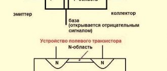
The field effect transistor consists of the following elements:
- n-channel, which has a silicon substrate with p-conductivity;
- n-regions, which are obtained by adding impurities to the substrate;
- insulating the gate from the dielectric channel.
Pins are connected to n-areas. Current flows from source to drain through the transistor thanks to the power supply. The amount of current is controlled by the insulated gate of the transistor.
When working with a transistor component, you must consider its sensitivity to the effects of an electric field . Such elements should be stored with the terminals short-circuited with foil, and before soldering they will need to be short-circuited with wire. Soldering of transistor elements is carried out using a soldering station that provides protection against static electricity.
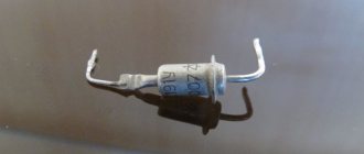
Before deciding how to test a mosfet with a multimeter, you need to determine its pinout. The imported device has marks corresponding to the terminals of the transistor. In this case, the letter G denotes the gate of the device, S is the source, and the designation D refers to the drain.
What malfunctions occur
Field-effect transistors can be overloaded with current during testing and, as a result of overheating, become faulty.
Important! They are vulnerable to static voltage. During the work, you need to ensure that it does not fall on the part being tested.
When working as part of a circuit, a breakdown may occur, as a result of which the field-effect transistor becomes faulty and must be replaced. It can be detected by the low resistance of pn junctions in both directions.
You can determine how efficient a transistor is by testing it with a digital multimeter.
Pin assignment
This should be done as follows (for example, the widely used M-831 model is used, a field-effect transistor with an n-type channel is considered):
- The multimeter must be switched to diode test mode. It is marked on the panel with a schematic diagram of a diode.
- Two probes are attached to the device: black and red. There are three slots on the front panel. Black is set to the bottom, red to the middle. The first of them corresponds to the negative pole, the second to the positive pole.
- It is necessary to determine on the field-effect transistor being tested which outputs correspond to the source, gate and drain.
- Some models additionally have an internal diode that protects the part from overload. First you need to check how it works. To do this, the red wire is connected to the source, and the black wire to the drain.
You may be interested in Checking a capacitor with a multimeter
Checking the diode in the forward direction
A value within the range of 0.5-0.7 should appear on the indicator. If the wires are swapped, the screen will indicate one, which means that no current flows in that direction.
Diode test in reverse direction
- Next, the functionality of the transistor is checked.
If you connect the probes to the source and drain, then the current will not pass through them. To open the shutter. A positive voltage must be applied to the gate. It must be taken into account that a positive potential is applied to the red probe from the multimeter. Now it is enough to connect it to the gate, and the black one to the drain or source, so that the transistor begins to pass current.
Channel opening
Now, if the red wire is connected to the source, and the black wire to the drain, then the multimeter will show a certain voltage drop value, for example, 60. If you connect it the other way around, the indicator will be approximately the same.
If a negative potential is applied to the gate, this will turn off the transistor in both directions, but the built-in diode will work. If the field switch does not close, this indicates its malfunction.
Checking the p-channel mofset is done in a similar way. The difference is that when testing where previously a red probe was used, a black one is now used and vice versa.
Operation of a field-effect MOS transistor
P-channel serviceability
The serviceability of the p-channel element is checked using the same method as for the n-channel type. The difference is that the red probe must be connected to the minus of the multimeter, and the black wire must be connected to the plus of the device.
Thus, the following conclusions can be drawn regarding field-effect transistor components and test procedures:
- Field elements of the MOSFET variety are widely used in radio electronics, technology and other areas related to practical electronics;
- Checking the performance of transistor elements is most convenient and best done using a multimeter - by following a certain step-by-step method;
- Testing p-channel and n-channel transistor components is carried out using the same methods, but it is necessary to reverse the polarity of the multimeter leads.
Field effect transistor components are very popular in various technical and electronic devices. But for high-quality and durable operation, periodic checking of mosfet transistors using a multimeter is required. By following all the methods described above, you can save significant financial costs associated with replacing and repairing field-effect transistors.
Recently I have been working from home doing electronic repairs. Repairing both equipment of friends and purchased from a local forum (Avito and Yule), with the aim of selling it. I worked on everything I had enough experience and knowledge for: from household audio-video to computer equipment.
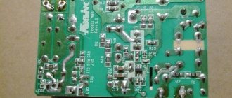
Recently I decided to go through the motherboards, of which there were a decent amount of them, the repair of which was not carried out immediately and which were postponed until better times. I counted four of them and all of them had similar breakdowns - short-circuited mosfets or, in other words, broken transistors in the processor power circuits. These are the same well-known squares, field-effect transistors in planar SMD design, usually located on the board to the left of the processor.
CPU power supply mosfets
Due to the fact that the processor consumes a fairly large amount of energy, which it dissipates as heat into the surrounding space, thereby heating the motherboard and the parts installed on it, it requires good cooling. For 2-core processors, the thermal package is usually 65-89 watts, for 4-core processors – 95 watts and higher.
CPU power chokes
To ensure that the electrolytic capacitors installed along the processor power supply circuits and located next to the processor radiator (cooler) do not swell from overheating, it is necessary to effectively remove the heat generated during processor operation, in other words, an effective cooling system is required. But let's get back to the essence of the repair.
Read also: Dovetail guides for machine tools
Mosfet transistor photo
If the cooling system fails, then in addition to the capacitors, the mosfets installed on the board and the transistors of the multiphase processor power system also heat up. The number of power phases ranges from three on budget motherboards, to 4-5 or more in more expensive, top-end gaming motherboards.
What happens when one of these squares, mosfets field-effect transistors, is broken? Many PC users have probably encountered a similar breakdown: you press the power button on the system unit case, the cooler twitches, tries to start rotating and stops, and when you try to turn it on again, everything happens again.
4 pin processor power cable
What does this mean? That there is a short circuit somewhere in the processor power circuits, but most likely one of these very mosfets is broken. How can you try to determine one of the options in the simplest way, whether this is your case, accessible even to a schoolchild who practically does not know how to handle a multimeter?
4 pin connector pinout
If, with the processor installed, you disconnect the 4 pin additional processor power connector on the motherboard and look at the colors where we have the yellow wire +12 volts, and the black wire, ground, or GND, and set the audio dialing mode on the multimeter to ring on this connector of the motherboard between A beep will sound with the yellow and black wires, this means that one or more mosfets are broken.
Mounting the transistor on the motherboard
But how can we determine which of the mosfets, which power phase is broken, because the mosfets of all processor power phases will ring as if they are all in a short circuit - look at the diagram, because they are in parallel and will ring when they break through low-resistance power chokes? In this case, the easiest way is to unsolder one leg of the throttle or if the throttle is in the housing, and for me personally it would be much more convenient, the entire throttle.
When taking measurements with a multimeter on mosfets, the processor must be removed, since it has low resistance, which can be misleading during measurements. So, by removing the inductor from the circuit, we eliminate the resistance of all parallel-connected radio components that always influences the correctness of the measurement results. Resistance, as you know, is always calculated in a parallel connection, according to the rule “less than less”.
Processor power supply
In other words, the total resistance of all radio components connected in parallel will be less than the resistance of the part that has the least resistance in our circuit when connected in parallel.
Field effect transistor - diagram image
So, as we see from the diagram, if one of the mosfets is broken, it will, with its low-resistance resistance, bypass all other power phases. And by removing all the chokes, we thereby disconnect all parallel circuits into separate circuits, in which the remaining phases cease to influence the measurement results in the circuit being tested.
So, the culprit of the short circuit (short circuit) of the power supply circuit has been found, now we need to eliminate it. How to do this, since not all novice radio amateurs have a soldering gun in their home workshop? First, we need to dismantle and unsolder the electrolytic capacitors that are usually installed closely from the board, which will interfere with us during dismantling and also really do not like overheating.
Soldering iron EPSN 40 watt photo
After which their service life is usually sharply reduced. The dismantling of capacitors itself, if you take into account some nuances, can be easily done using any soldering iron with a power of 40-65 watts. It is advisable to have a processed tip, sharpened into a cone. I myself have a Lukey soldering station and a soldering hair dryer, but to dismantle capacitors I use a regular 40-watt EPSN soldering iron with a tip sharpened into a sharp cone.
Soldering hair dryer photo
True, there is one nuance here - for ease of work, I use a purchased dimmer on a cord, which is produced for incandescent lamps but is also excellent for regulating the power of a soldering iron. All that remains is to attach the socket for the extension cord to it, which comes with a cord attachment, and the camping dimmer is ready.
Dimmer for 220V cord
The cost of this dimmer was quite modest, only about 130 rubles, I also saw similar dimmers on Ali Express - this is for those who do not have access to radio stores with a good selection of radio products. But let’s return to dismantling first the capacitors and then the mosfets.
POS 61 solder with rosin
If with capacitors this procedure does not have any difficulties, with the exception of one trick used to reduce the overall melting point of lead-free solder, which, as is known, has a higher melting point than the solder used for soldering POS-61 electronics.
So, we take tubular solder with POS-61 flux, preferably with a diameter of no more than 1-2 millimeters, bring it to the capacitor contact on the back side of the board and, heating it, melting it, deposit solder on each of the two capacitor contacts. For what purpose do we perform these actions?
- Goal one: by diffusion of alloys mixing lead-free solder and POS-61, we lower the overall melting temperature of the resulting alloy.
- Goal two: in order to transfer heat from the soldering iron tip to the contact as efficiently as possible, we, relatively speaking, heat the contact with a small drop of solder, transferring heat much more efficiently.
- And finally, the third goal: when we need to clean the hole in the motherboard after dismantling the capacitor for subsequent installation, no matter when replacing the capacitor or installing it back, as in this case of the same capacitor, we facilitate this process by piercing a hole in the molten solder, having previously reduced the overall the temperature of the alloy inside our contact.
Read also: DIY plasterboard profile cutter
Here we need to make one more digression: for this purpose, many radio amateurs use various improvised means, some a wooden toothpick, some a sharpened match, some other objects.
Aluminum Tapered Bar
I was luckier in this regard - a conical aluminum rod was left over from Soviet times from one of the installers, which greatly facilitates the performance of this work.
With its help, we just need to warm up the contact and insert the rod deeper into the contact hole. Moreover, this action should be carried out without fanaticism, always remembering that the motherboard is a multilayer board, and the contacts inside have metallization, in other words, metal foil, tearing off which if you did not warm up the contact enough or sharply inserted an object with which you cleaned the hole in the contact, you can cause a motherboard or any other device having a similar complex printed circuit board design to become a device beyond repair.
So, all difficulties have been overcome, the capacitors have been successfully dismantled, we finally move on to replacing our mosfets, that is, the goal of our article. Actually, any procedure for replacing a part involves three stages: first dismantling, then preparing the board for subsequent installation, and finally the installation itself of a new part or one previously removed from the donor board in this or another way.
If you have a soldering gun, everything is simple here, we set the temperature recommended in the Datasheet for dismantling our part, which it will easily tolerate and will not become unusable, apply flux and solder the part. Installation if you have a hairdryer is also possible with its help by first applying flux. Installation is also possible using a soldering iron, either from a soldering station, or in the absence of one, using a 25-watt EPSN soldering iron with a sharpened tip; I usually use a soldering iron for installation.
Under no circumstances should you use soldering irons with a power of 40-65 watts, especially grandfather’s ax-shaped ones for mounting mosfets on a board (at least in the absence of a dimmer with which we can lower the temperature of the soldering iron tip). At the beginning of the article there was a mention of the option of dismantling mosfets for beginners who do not have a soldering hair dryer in the workshop, now we will analyze this option in more detail.
Wood alloy photo
There is such a wonderful invention - Rose and Wood alloys, especially for Wood's alloy, which has a lower melting point than Rose's alloy. These alloys have a very low melting point, about 100 degrees, plus or minus I won’t specify, it’s not that important. So, having bitten off a small drop of any of these alloys with side cutters and, of course, applying flux, we put this drop on the contacts of our mosfet and, heating it with a soldering iron tip, deposit it on the contacts.
Moreover, on the side of the drain, the middle contact which has a large area of contact with the board, we apply significantly more of this alloy. The purpose of this operation? Just as in the case of applying the POS-61 alloy, we reduce, and this time much more significantly, the overall melting temperature of the solder, thereby facilitating dismantling conditions.
Dismantling microcircuits without a hair dryer
This operation requires care from the performer so that during dismantling he does not tear off the contacts from the board, so if we feel that they have not warmed up enough, and heating is required by alternately quickly changing the soldering iron tip at these three contacts, slightly shaking the part with tweezers, of course, without fanaticism. After performing this operation 3-5 times, you will automatically feel when the contacts of the part are sufficiently warmed up, and when they are not yet.
Dismantling using braid
This dismantling method has one drawback, but if you have experience, this does not become a problem: overheating when removing mosfets from donor boards. If you purchased a new mosfet from a radio store and are sure that you are dismantling the broken mosfet, overheating becomes not very critical. After dismantling, you should definitely make sure whether the short circuit on the mosfet contacts on the board has disappeared, rarely, but unfortunately, sometimes it happens that our supposedly broken mosfet had nothing to do with it, but the driver or PWM controller influenced the measurement results, which came in disrepair. In this case, it will be impossible to do without the help of a soldering hair dryer.
Read also: Gas cylinders for burners
Housing SO-8 microcircuit
Personally, I have dismantled microcircuits in the SO-8 package many times using this method, sometimes using a 65-watt soldering iron on the contacts with the polygons and slightly reducing its power with a dimmer. The result, if the performer is careful, is almost 100% successful. For SMD microcircuits with a larger number of legs, this method is unfortunately useless, because heating a larger number of legs without special nozzles is problematic and there is a very high probability of tearing off the contacts on the board.
I had this opportunity, once there was an urgent repair of an LCD TV in a small workshop that did not have soldering equipment; the microcircuit in the SO-14 case was dismantled, but unfortunately, along with two nickels of contacts. This did not become a problem - the missing connections were thrown by the MGTF wire from the nearest contacts connected by tracks with broken contacts. The TV was brought back to life, there were no complaints from the client.
With this method of dismantling, “snot” always remains on the board - lumps of solder, which are easily removed from the board first using a desoldering pump, then you should pass the dismantling braid over the contacts, soaked in flux. When installing and dismantling, I always use a self-prepared saturated alcohol-rosin flux, obtained by dissolving Aseptolin in 97% pharmaceutical alcohol denatured alcohol, finely crushed rosin into powder.
Then you need to let the flux solution sit for two or three days until the rosin dissolves in alcohol, periodically shaking it many times, not allowing it to precipitate. I apply this flux using a nail polish brush, respectively, pouring the resulting flux into a bottle cleaned of traces of varnish with 646 solvent. When using this flux, there is much less dirt on the board than from any Chinese fluxes, such as BAKU or RMA-223.
Making alcohol rosin flux
We remove the one that still remains from the board using 646 solvent and a regular brush for labor lessons. This method, compared to removing traces of flux even with 97% alcohol, has a number of advantages: it dries quickly, dissolves better and leaves less dirt. I recommend it to everyone as an excellent budget solution.
646 solvent photo
The only thing I would like to note is: be careful with plastic parts, do not apply to graphite contacts, such as those found on boards of remote controls and potentimeters, and never rush, let the board dry thoroughly, especially if there is a risk of solvent flowing under nearby SMD and especially BGA microcircuits.
Graphite contacts of the remote control board
Thus, the process of installing and dismantling mosfets on motherboards is not something extremely difficult, if you have more or less direct hands, and can be performed by any radio amateur with little repair experience. Happy repairs to everyone – AKV.
MOSFET transistors have recently become more and more popular. They can serve as a good replacement for relays and bipolar transistors.
To save money and not have to run to the store again, MOSFET transistors can be removed from a non-working motherboard or some control module.
But how can you check the functionality of these radio components? To do this, we need only one device - a tester. Every radio amateur (even a beginner) must have one!
The vast majority of testers have a “continuity” mode combined with checking the diode voltage drop. This is the mode we switch the tester to.
Now let's look at the circuit of an N-channel MOSFET transistor.
There is a diode in the drain-source circuit. By the way, its presence is due to production technology. The tester can confirm the presence of this diode.
0.5V is the voltage drop across the internal Schottky diode. If you swap the probes, there should be a “break”.
Now you can check the shutter. The tester should show a “break” when testing gate-source and gate-drain, and the polarity of the probes does not matter.
But what’s interesting is that if you hold the black probe (“-“) at the source, and touch the gate with the red probe (“+”), the transistor will open. Which we can verify by checking the drain-source again.
The tester will show almost zero resistance.
Now let’s place the “+” probe on the drain and the black probe on the gate and check the drain-source. The tester will again show either a voltage drop across the diode or a “break”, i.e. the transistor has closed!
By the way, there is one more subtlety - if we open the transistor and measure the drain-source resistance, but not immediately, but after a while, then the tester will show a resistance other than zero. And the more time passes, the greater the resistance will be.
Why is this happening? And everything is very simple - the capacitance between the gate and drain is quite large (usually units of nanofarads) and when we open the MOSFET transistor, this capacitance is charged. And since the field-effect transistor is controlled by a field and not a current, the transistor will be open until the capacitor is discharged.
A P-channel MOSFET transistor can be tested using the same principle, only the gate polarity is different.
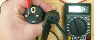
Instructions for dialing without soldering
To check whether the field-effect transistor is working, you need to unsolder it and test it with a multimeter. However, situations may arise when you need several such parts in the circuit and it is not known which of them are working and which are not. In this case, it is useful to know how to test a field-effect transistor with a multimeter without desoldering.
Digital multimeter
In this case, a test without desoldering is used. It gives an approximate result.
Important! After the presumably faulty element has been identified, it is disconnected and checked, obtaining accurate information about its performance. If it functions normally, it is installed in its original place.
Testing without desoldering is performed as follows:
- Before testing the field-effect transistor with a digital multimeter, disconnect the device from the electrical outlet or from the batteries. The latter are removed from the device.
- If the red probe is connected to the source, and the black probe to the drain, then you can expect that the multimeter will show 500 mV. If you can see this figure or one that exceeds it on the indicator, this indicates that the transistor is fully functional. If this value is much less - 50 or even 5 mV, then in this case a malfunction can be assumed with a high probability.
You might be interested in: Features of the Tesla Coil
With control pn junction
- If the red multimeter probe is moved to the gate, and the black one is left in the same place, then the indicator will show 1000 mV or more, which indicates the serviceability of the field-effect transistor. When the difference is 50 mV, this raises concerns that the part is damaged.
- If the black probe of the tester is placed on the source, and the red probe is placed on the gate, then for a working transistor you can expect 100 mV or more on the display. In cases where the figure is less than 50 mV, there is a high probability that the part being tested is inoperative.
It must be taken into account that the conclusions obtained without soldering are probabilistic in nature. These data allow us to draw preliminary conclusions about the field-effect transistors used in the circuit.
To check, they need to be unsoldered, checked and installed if the functionality is confirmed.
Preparing for work
Safe work rules
Mosfets are very vulnerable to static electricity. In this case, a breakdown may occur. To prevent this from happening, you need to remove it through testing.
When soldering, a situation is possible where the heat entering the transistor will lead to its damage. In this case, it is necessary to provide heat dissipation. To do this, just hold the transistor terminals with pliers during the soldering process.
Field workers are widely used in modern electronic devices. When a breakdown occurs, you need to know how to check the mosfet. It is possible to find out if it is working if you use a multimeter for this.
A little about the design
The field effect transistor consists of the following elements:
- n-channel, which has a silicon substrate with p-conductivity;
- n-regions, which are obtained by adding impurities to the substrate;
- insulating the gate from the dielectric channel.
Pins are connected to n-areas. Current flows from source to drain through the transistor thanks to the power supply. The amount of current is controlled by the insulated gate of the transistor.
When working with a transistor component, you must consider its sensitivity to the effects of an electric field . Such elements should be stored with the terminals short-circuited with foil, and before soldering they will need to be short-circuited with wire. Soldering of transistor elements is carried out using a soldering station that provides protection against static electricity.
Before deciding how to test a mosfet with a multimeter, you need to determine its pinout. The imported device has marks corresponding to the terminals of the transistor. In this case, the letter G denotes the gate of the device, S is the source, and the designation D refers to the drain.