Logic elements were invented to perform logical operations and solve logical problems using electronics. They are created using diodes, transistors and combined elements (diode-transistor). This logic is called diode logic (DL), transistor logic (TL) and diode-transistor logic (DTL). Both field-effect and bipolar transistors are used. In the latter case, preference is given to npn type devices, as they are faster.
Logic element "OR"
The diagram of the “OR” logic element is shown in Figure 1 a. Each input can receive a signal in the form of some voltage (one) or its absence (zero). Voltage will appear across resistor R even if it appears on any of the diodes.
Rice. 1
Elements or can have several logical inputs. If not all inputs are used, then those inputs that are not used should be connected to ground (grounded) to avoid the appearance of extraneous signals.
Figure 1b shows the designation on the electrical circuit of the element, and 1c shows the truth table.
Elementary logic gates
The main logical elements are AND, OR, NOT. All other elements are built on their basis.
Rice. 1. Graphic representation of the elements AND, OR, NOT
Inversion (NOT)
Inversion is a unary operation, that is, an element with one input. The logic gate does NOT implement logical negation. If a 1 signal is applied to the input of this element, then the output will be 0.
The truth table for this element is:
| A | NOT(A) |
| 0 | 1 |
| 1 | 0 |
Conjunction (I)
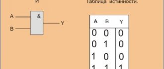
The AND gate is binary and performs logical multiplication. The result of the conjunction is equal to 1 only if two units are supplied to the inputs of this element. In all other cases, the result of the conjunction is zero.
Truth table for conjunction
| A | IN | A&B |
| 0 | 0 | 0 |
| 0 | 1 | 0 |
| 1 | 0 | 0 |
| 1 | 1 | 1 |
Disjunction (OR)
The binary OR gate implements the logical addition operation. The result of this operation is equal to zero in the case when zeros are supplied to the disjunction inputs. In other cases, the result is always equal to one.
Truth table for logical OR
| A | IN | A + B |
| 0 | 0 | 0 |
| 0 | 1 | 1 |
| 1 | 0 | 1 |
| 1 | 1 | 1 |
Logic gate "AND"
The element diagram is shown in Fig. 2. If at least one of the inputs has a signal equal to zero, then current will flow through the diode. The voltage drop across the diode tends to zero, and accordingly the output will also be zero. A signal can appear at the output only if all diodes are closed, that is, there will be a signal at all inputs. Let's calculate the signal level at the device output:
Fig.2
in Fig. 2 b – designation on the diagram, c – truth table.
Logic element "NOT"
A transistor is used in the “NOT” logic element (Fig. 3 a). when there is a positive voltage at the input x=1, the transistor opens and its collector voltage tends to zero. If x = 0, then there is no positive signal at the base, the transistor is closed, the current does not pass through the collector and there is no voltage drop across the resistor R, respectively, signal E will appear on the collector. The symbol and truth table are shown in Fig. 3 b, c.
Fig.3
Logic elements from the inside
Digital chips are designed for processing, converting and storing digital information. They are produced in series. Within each series there are groups of devices united by functional characteristics: logical elements, flip-flops, counters, elements of arithmetic devices (performing various mathematical operations), etc. The wider the functional composition of the series, the greater the capabilities a digital device made on the basis of microcircuits of this series can have. The microcircuits included in each series have a single design and technological design, a single supply voltage, and the same levels of logical 0 and logical 1 signals. All this makes microcircuits of the same series compatible.
The basis of each series of digital chips is a basic logic element. As a rule, basic logic elements perform AND-NOT or NOR-NOT operations and, according to the principle of construction, are divided into the following main types: diode-transistor logic elements (DTL). resistive-transistor logic (RTL), transistor-transistor logic (TTL), emitter-coupled transistor logic (ECTL), microcircuits based on the so-called complementary MIS structures (CMOS). CMOS elements of digital microcircuits use pairs of MOS transistors (with a metal-dielectric-semiconductor structure) - with p- and n-type channels. Basic elements of other types are made on bipolar transistors.
In amateur radio practice, the most widely used microcircuits are the TTL series and KMDP. Figure 1 shows the circuit diagram of a basic TTL NAND gate. The multi-emitter transistor VT1 is switched on at the input of the element. If high-level voltages are applied to all its emitters, the emitter junction of the transistor will be closed. At the same time the current. flowing through resistor R1 and the collector junction of transistor VT1 will open transistor VT2. The voltage drop across the resistor RЗ will be sufficient to open the transistor VT5. The voltage at the collector of transistor VT2 is such that transistor VTZ is closed, and transistor VT4 is correspondingly closed. As a result, a low-level voltage corresponding to logical 0 will appear at the output of the element. If a low-level voltage is applied to at least one of the inputs of the element, then the emitter junction of transistor VT1 will open, and transistors VT2 and VT5 will be closed. Transistor VTZ will open due to the current flowing through resistor R2 and will enter saturation mode. Accordingly, transistor VT4 will open, and a high-level voltage corresponding to logical 1 will appear at the output of the element. Consequently, the considered element performs the AND-NOT function. The TTL series microcircuits also include a NAND logic element without a collector load in the output stage. This is the so-called open collector NAND element. It is designed to operate on an external load, which can be electromagnetic relays, indicator devices, etc.; open-collector circuits are also used in data transmission buses in cases where two or more outputs are connected to one physical line, Figure 1.
Picture 1
Recall that the CMOS structure is an ideal voltage switch. Such a switch contains two MOS transistors with p- and n-type channels. When a high level voltage is applied to the input of the switch, the n-channel transistor opens and the p-channel one closes. Figure 2 shows the circuits of the basic elements of AND-NOT (a) and NOR-NOT (b) KMDP microcircuits. A low level voltage (logical 0) will be at the output of the AND-NOT element only when high level voltages (logical 1) are simultaneously applied to all inputs of X1-XZ. If the voltage at at least one of the inputs (for example, X1) is low, then the n-channel transistor VT6 will close, and the p-channel transistor VT1 will open, through the channel of which the output of the element is connected to the power source. Thus, the output will have a high-level voltage corresponding to logical 1. To implement the basic logical element OR-NOT on CMOS structures, sections of the circuit containing transistors connected in series and in parallel should be swapped in Figure 2, b.
Figure 2
TTL chips are designed for a power supply voltage of 5 V±10%. Most of the microcircuits based on CMOS structures operate stably at a supply voltage of 3-15 V, some at a voltage of 9 V±10%. The logical levels 0 and 1 should differ as much as possible. There is a threshold logical 1 U1pore - the lowest high-level voltage at the input of the microcircuit, at which the output voltage changes from the logical level 0 to a logical level 1, as well as a threshold voltage of logical 0 U0por - the highest low-level voltage at the input of the microcircuit, at which the output voltage changes from logical level 1 to logical level 0.
Before moving on to a detailed examination of the most common series of microcircuits and digital devices based on them, let us dwell on the main parameters of logic elements. These include the power supply voltage, logical 0 and logical 1 voltage levels, load capacity, noise immunity and performance, and power consumption.
For TTL series microcircuits U1por = 2.4 V; U0por =0.4 V. Low and high level voltage at the output of TTL microcircuits U1out>=2.4V, U1out<=0.4V.
For microcircuits based on CMOS structures U1por>0.7* Upit, U0pore>0.3* Upat the same time, deviations of the output voltages U0out and U1out from zero and the power source voltage, respectively, reach only a few tens of millivolts. The ability of an element to operate on a certain number of inputs of other elements without additional matching devices is characterized by load capacity. The higher the load capacity, the fewer elements may be needed when implementing a digital device. However, as the load capacity increases, other parameters of the microcircuits deteriorate: performance and noise immunity decrease, and power consumption increases. In this regard, various series of microcircuits contain so-called buffer elements with a load capacity several times greater than that of the main elements. The load capacity is quantified by the number of unit loads that can be simultaneously connected to the output of the microcircuit. In turn, the unit load is the input of the main logical element of this series.
The output branching factor for most logic elements of the TTL series K155 is 10, for microcircuits of the K561 KMDP series - up to 100. The noise immunity of basic logic elements is assessed in static and dynamic modes. In this case, static noise immunity is determined by the voltage level supplied to the input of the element relative to the logical levels 0 and 1, at which the state at the output of the circuit does not change. For TTL elements, static noise immunity is at least 0.4 V, and for microcircuits of the KMDP series, at least 30% of the supply voltage. Dynamic noise immunity depends on the shape and amplitude of the interference signal, as well as on the switching speed of the logic element and its static noise immunity. The dynamic parameters of basic elements are assessed, first of all, by their performance. Quantitatively, performance can be characterized by the maximum operating frequency, i.e., the maximum switching frequency of a trigger made on these basic elements. The maximum operating frequency of the K155 series TTL microcircuits is 10 MHz. and microcircuits of the K176 and K561 series on KMDP structures are only 1 MHz. Performance is determined in the same way as the average signal propagation delay time.
Figure 3
tzd.r.av.=0.5(t1.0zd.r+t0.1zd.r), where t1.0zd.r and t0.1zd.r are the signal propagation delay times when turning on and off, Figure 3.
The average signal propagation delay time is a more universal parameter of microcircuits, since knowing it. You can calculate the performance of any complex logic circuit by summing tz.r.sr for all series-connected microcircuits. For K155 series microcircuits tz.r.sr is about 20 ns, and for K176 series microcircuits - 200 ns. The power consumed by the microcircuit in static mode is different at the levels of logical zero (P0) and logical one at the output (P1). In this regard, the average power consumption is measured Рср=(Р0+Р1)/2. The static average power consumption of basic elements of the K 155 series is several tens of milliwatts, and for elements of the K176 and K561 series it is more than a thousand times less. Therefore, if it is necessary to build digital devices with low current consumption, it is advisable to use microcircuits based on KMDP structures. However, it should be taken into account that when operating in dynamic mode, the power consumed by logic elements increases. Therefore, in addition to Рср, the power Рdin is also specified, measured at the maximum switching frequency. Something to keep in mind. that with increasing speed, the power consumed by the microcircuit increases
Logic element "OR-NOT"
When creating various circuits using logical elements, combined elements are often used. Such elements combine several functions. The schematic diagram is shown in Fig. 4 a.
Fig.4
Here diodes D1 and D2 play the role of an “OR” element, and the transistor plays the role of an inverter. Designation of the element in the diagram and its truth table Fig. 4b and c respectively.
Logic element "AND-NOT"
The diagram is shown in Fig. 5 a. Here diode D3 acts as a filter, so to speak, to avoid signal distortion. If no signal is applied to input x1 or x2 (x1=0 or x2=0), then current will flow through diode D1 or D2. The drop across it is not zero and may be sufficient to open the transistor. The consequence may be a false positive and at the output we will get zero instead of one. And if D3 is included in the circuit, then a significant part of the voltage of the diode open at the input will drop across it, and practically nothing comes to the base of the transistor. Therefore, it will be closed, and the output will be one, which is required if there is a zero at any of the inputs. In Fig. 5b and c show the truth table and circuit designation of this device.
Fig.5
Logic elements are widely used in electronics and microprocessor technology. Many control systems are built using these devices.
Let's consider the simplest logical elements
Logic elements
Any digital device - a personal computer, or a modern automation system consists of digital integrated circuits (ICs) that perform certain complex functions. But to perform one complex function, it is necessary to perform several simple functions. For example, the addition of two one-byte binary numbers occurs inside a digital chip called a “processor” and is performed in several stages by a large number of logic elements,
located inside the processor. Binary numbers are first stored in the buffer memory of the processor, then rewritten into special “main” registers of the processor, then they are added, the result is stored in another register, and only after that the result of the addition is output through the buffer memory from the processor to other computer devices.
The processor consists of functional units: input-output interfaces, memory cells - buffer registers and “accumulators”, adders, shift registers, etc. These functional units consist of the simplest logical elements, which in turn consist of semiconductor transistors, diodes and resistors. When designing simple trigger and other electronic pulse circuits, complex processors cannot be used, but using transistor cascades is “last century”. logical elements come to the rescue.
.
Logic elements
, these are the simplest “cubes”, components of a digital microcircuit that perform certain logical functions.
At the same time, a digital microcircuit can contain from one to several units, tens, ... and up to several hundred thousand logical elements, depending on the degree of integration. In order to understand what logical elements are
, we will consider the simplest of them. And then, as we build up our knowledge, we’ll deal with more complex digital elements.
Let's start with the fact that the unit of digital information is “one bit”. It can take two logical states - a logical zero “0” when the voltage is zero (low level), and a logical one state “1” when the voltage is equal to the supply voltage of the microcircuit (high level). Since the simplest logic element is an electronic device, this means that it has inputs (input pins) and outputs (output pins). There may be one input and output, or there may be more. In order to understand the principles of operation of the simplest logical elements, a “truth table”
. In addition, to understand the principles of operation of logical elements, the inputs, depending on their number, are designated: X1, X2, ... XN, and the outputs: Y1, Y2, ... YN. The functions performed by the simplest logic elements have names. As a rule, a number indicating the number of inputs is placed in front of the function. The simplest logic elements always have only one output.
The simplest logical elements AND and OR can be built on the basis of diode switches. A transistor switch with inverting properties is usually used as a NOT element.
Let's consider the simplest logical elements
— "NOT"
– negation function (signal inversion).
That is why it is often called “inverter”
. Graphically, inversion is indicated by an empty circle around the output of the element (microcircuit). Usually the inversion circle is placed at the output, but in more complex logic elements, it can also be at the input. The graphic designation of the “NOT” element and its truth table are presented in the figure.
The NOT element always has one input and one output. According to the truth table, if there is a logical zero at the input of an element, the output will be a logical one. And vice versa, if there is a logical one at the input, the output will be a logical zero. The number “1” inside the rectangle denotes the “OR” function; it is customary to draw it inside the rectangle of the “NOT” element, but this means absolutely nothing.
The designation D1.1 means that D is a digital logic element, 1 (first) is the number of the microcircuit in the general circuit, 1 (second) is the number of the element in the microcircuit. Other logical elements are deciphered in the same way.
Often, to distinguish digital microcircuits from analog microcircuits, two-letter designations are used: DD
– digital chip,
DA
– analog chip. Subsequently, we will not focus on this designation, but will return only when it is necessary.
The most common “transistor-transistor logic” (TTL) microcircuit that performs the “NOT” function is the K155LN1 integrated circuit (IC), which contains six “NOT” elements inside. The numbering of the pins of this microcircuit is shown on the right.
— "AND"
– logical multiplication function (if all inputs are one, then the output will be one, otherwise, if at least one input is zero, then the output will always be zero).
In algebra-logic, the element “AND” is called “conjunctor”
. The graphic designation of the “2I” element and its truth table are presented on the left.
When a “0” signal is applied to all inputs, all diodes will open, and current generated by the power source and closed through the signal sources will flow through them and resistor R. Since the resistance of the resistor R is significantly greater than the resistance of the open diode, practically all “E” drops across it, and the output voltage is close to zero.
If the voltage at one of the inputs corresponds to logical “1” (E˃5V), then the corresponding diode closes. However, the rest are open and therefore the output is "0".
If the voltage at all inputs corresponds to logical “1” (E˃5V), then all diodes close, the current through resistor R will be zero and Uout = E(5V), i.e. will be equal to logical "1".
Element name "2I"
denotes that it has two inputs and performs the
AND
.
“&”
icon is drawn inside the rectangle of the microcircuit , which in English means “AND” (translated into Russian as “I”).
According to the truth table, it follows that the output of the “AND” element will be a logical one only in one case - when there is a logical one at both inputs. If at least one input is zero, then the output will be zero.
The most common transistor-transistor logic (TTL)
, performing the “2I” function is an integrated circuit (IC) K155LI1, inside of which there are four “2I” elements. The numbering of the pins of this microcircuit is shown on the right.
In order to make it clearer to you what “2I”, “3I”, “4I”, etc. are, I will give a graphic designation and truth table for the element “3I”.
According to the truth table, it follows that the output of the “3I” element will be a logical one only if there is a logical one at all three inputs. If at least one input is logical zero, then the output of the element will also be logical zero. The most common TTL microcircuit that performs the “3I” function is the K555LI3 microcircuit, inside of which there are three “3I” elements.
— "NAND" (NAND)
– function of logical multiplication with negation (if all inputs are one, then the output will be zero, otherwise the output will always be one).
To obtain a logical NAND element, it is necessary to add a transistor stage of the NOT circuit to the diode part of the “AND” circuit.
Ds ensures reliable locking of the transistor at a low but positive potential at the lower end of R1, corresponding to the logical “0” of the AND element. This is an example of a diode-transistor logic circuit - DTL.
The graphic designation of the element “2AND-NOT” and its truth table are shown on the left.
According to the truth table, it follows that the output of the “2I-NOT” element will be logical zero only if there is a logical one at both inputs. If at least one input is zero, then the output will be one.
The most common TTL microcircuit that performs the “2I-NOT” function is the K155LA3 IC, and CMOS (complementary metal oxide semiconductor)
– ICs K561LA7 and K176LA7, inside of which there are four “2I-NOT” elements. The numbering of the pins of these microcircuits is shown on the right.
By comparing the truth tables of the “2I-NOT” element and the “2I” element, you can guess the equivalence of the circuits:
By adding the “NOT” element to the “2I” element, we got the “2I-NOT” element. This is how we can assemble a circuit if we need a “2I-NOT” element, but we only have the “2I” and “NOT” elements at our disposal.
And vice versa:
By adding the “NOT” element to the “2I-NOT” element, we got the “2I” element. This is how we can assemble a circuit if we need the “2I” element, but we only have at our disposal the “2I-NOT” and “NOT” elements.
Similarly, by connecting the inputs of the “2AND-NOT” element, we can obtain the “NOT” element:
Please note that a new element has been introduced in the designation of elements - a hyphen separating the right and left parts in the name “2I-NOT”. This hyphen is an indispensable attribute when inverting the output (“NOT” function).
— "OR" (OR)
– logical addition function (if at least one of the inputs is one, then the output is one, otherwise the output will always be zero). In algebraic logic, the “OR” element is called a “disjunctor”. The graphic designation of the “2OR” element and its truth table are shown on the left.
The most common TTL microcircuit that performs the “2OR” function is the K155LL1 IC, inside of which there are four “2OR” elements. The numbering of the pins of this microcircuit is shown on the right.
Suppose that we need an element in the circuit that performs the “2OR” function, but we only have at our disposal the “NOT” and “2AND-NOT” elements, then we can assemble a circuit that will perform the “2OR” function:
— "OR-NOT" (NOR)
– selection function (if at least one of the inputs is one, then the output is zero, otherwise the output will always be one). As you understand, the “OR-NOT” element performs the “OR” function, and then inverts it with the “NOT” function.
The graphic designation of the “2OR-NOT” element and its truth table is shown on the left.
The most common TTL microcircuit that performs the “2OR-NOT” function is the K155LE1 IC, and the CMOS microcircuits are K561LE5 and K176LE5, inside of which there are four “2OR-NOT” elements. The numbering of the pins of these microcircuits is shown on the right.
Suppose that we need an element in the circuit that performs the “2OR-NOT” function, but we only have at our disposal the elements “NOT” and “2AND-NOT”, then we can assemble the following circuit that will perform the “2OR-NOT” function :
By analogy with the “2AND-NOT” element, by connecting the inputs of the “2OR-NOT” element we can obtain the “NOT” element:
— Exclusive OR (XOR)
— a function of inequality of two inputs (if both inputs of an element have identical signals, then the output is zero, otherwise the output will always be one). The operation it performs is often called "addition modulo 2".
The graphic designation of the “Exclusive OR” element and its truth table are shown on the left.
The most common TTL microcircuit that performs the “Exclusive OR” function is the K155LP5 IC, and the CMOS microcircuits are K561LP2 and K176LP2, inside of which there are four “Exclusive OR” elements. The numbering of the pins of these microcircuits is shown on the right.
Suppose that we need an element in the circuit that performs the “Exclusive OR” function, but we only have “2AND-NOT” elements at our disposal, then we can assemble the following circuit that will perform the “ Exclusive OR”
:
In the digital circuitry of processors, the main function is “Summation of binary numbers”, therefore a complex logical element is “Adder”
is an integral part of the arithmetic-logical device of any processor without exception.
An integral part of the adder is a set of logical elements that perform the function “Exclusive OR with remainder carryover”
. What it is? In accordance with the science of Computer Science, the result of adding two binary numbers, two units of the same digit give zero, and a “carry unit” is formed to the next most significant digit, which participates in the summation operation in the most significant digit. To do this, another “transfer” pin is added to the circuit - “P”.
A graphical representation of the "Exclusive OR with Carry" element and its truth table are presented.
This function of adding single-digit numbers is usually not used in simple devices, and, as a rule, is integrated into one microcircuit - an adder, with a minimum number of digits - four, for adding four-bit numbers. Due to weak demand, the industry does not produce such logic elements. Therefore, if necessary, the “Exclusive OR with carry” function can be assembled according to the following scheme from the elements “2AND-NOT” and “2OR-NOT”, which is actively used both inside simple adders and in all complex processors (including Pentium, Intel-Core, AMD and others that will appear in the future):
The above logical elements perform static functions, and on their basis more complex static and dynamic elements (devices) are built: flip-flops, registers, counters, encoders, decoders, adders, multiplexers.