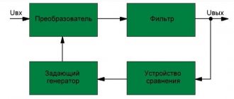
Operating principle of an electronic trigger.
The word trigger (trigger) in English means trigger. The function of a trigger is to instantly switch from one stable state to another, under the influence of an external, control factor. There are pneumatic, mechanical and relay trigger circuits. But electronic circuits, in terms of reliability and, most importantly, speed, are certainly unrivaled. The electronic trigger circuit consists of two amplification stages and, in essence, is a type of multivibrator.
The output of each stage is connected to the input of the other, but not through capacitors, as in a conventional symmetrical multivibrator, but through resistors. The values of these resistors are selected so that a cascade with a fully open transistor reliably turns off the transistor of another cascade. If you apply supply voltage to the trigger, then both cascades begin to “fight” with each other, trying to close each other.
No matter how similar the transistors are in terms of characteristics, one of them (let’s assign number 1 to it) will definitely turn out to be “stronger” and will close the other (for convenience, let’s designate it as number 2) Everything happens very quickly, it looks like transistor 1 instantly turns on, and the other (2) closed. The trigger can remain in this state for a very long time. We can call it the 1st stable state.
If you apply a voltage pulse to the input of a closed cascade (2) sufficient to open it for a short time, then when it opens it will “inhibit” cascade 1, which has been in the open state until that moment. Having closed, cascade 1 ceases to lock cascade 2, and it will remain open. Thus, the cascades will change places, the trigger will be in the 2nd stable state.
It can remain in this state for a very long time if an opening pulse is not applied to closed cascade 1. Cascade 1 opens, cascade 2 is inhibited and the trigger returns to its original state (1). It turns out that our trigger has two stable states and two control inputs, by applying pulses of sufficient amplitude to which these states can be changed.
Brief theoretical information
Triggers are designed to store binary information. The use of triggers makes it possible to implement RAM devices (that is, memory in which information is stored only for the duration of calculations).
However, flip-flops can also be used to build some digital memory devices, such as counters, serial-to-parallel converters, or digital delay lines.
RS trigger
The main trigger on which all other triggers are based is the RS trigger. The RS trigger has two logical inputs:
- R – setting 0 (from the word reset);
- S – setting 1 (from the word set).
The RS trigger has two outputs:
- Q – straight;
- Q - reverse (inverse).
The state of the trigger is determined by the state of the direct output. The simplest RS flip-flop consists of two logic elements covered by cross positive feedback.
Let's look at how the trigger works:
Let R=0, S=1. The lower logical element performs the logical OR-NOT function, i.e. 1 at any of its inputs leads to the fact that its output will have a logical zero Q=0. The output Q will be 1 (Q=1), because zeros are supplied to both inputs of the upper element (one zero from input R, the other from output). The trigger is in a single state. If we now remove the setting signal (R=0, S=0), the situation at the output will not change, because Although the lower input of the lower logic gate will receive a 0, its upper input will receive a 1 from the output of the upper logic gate.
It will be interesting➡ How a three-phase rectifier works
The flip-flop will remain in the single state until a reset signal is received at the R input. Let now R=1, S=0. Then Q=0, a =1. The trigger switched to “0”. If after this you remove the reset signal (R=0, S=0), then the trigger will still not change its state. To describe the operation of a trigger, a table of states (transitions) is used. Let's denote:
- Q(t) – state of the trigger before the arrival of control signals (changes at inputs R and S);
- Q(t+1) – trigger state after changes at inputs R and S.
Transition table of RS flip-flop in NOR basis
| R | S | Q(t) | Q(t+1) | Explanations |
| Information storage mode R=S=0 | ||||
| 1 | 1 | |||
| 1 | 1 | Unit setting mode S=1 | ||
| 1 | 1 | 1 | ||
| 1 | Zero setting mode R=1 | |||
| 1 | 1 | |||
| 1 | 1 | * | R=S=1 prohibited combination | |
| 1 | 1 | 1 | * |
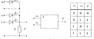
An RS trigger can also be built using “AND-NOT” elements (Figure 2.2).
Inputs R and S are inverse (active level “0”). The transition (switching) of this trigger from one state to another occurs when one of the inputs is set to “0”. The combination R=S=0 is prohibited.
Transition table of RS flip-flop in the “2AND-NOT” basis
| R | S | Q(t) | Q(t+1) | Explanations |
| * | R=S=0 prohibited combination | |||
| 1 | * | |||
| 1 | Zero setting mode R=0 | |||
| 1 | 1 | |||
| 1 | 1 | Unit setting mode S=0 | ||
| 1 | 1 | 1 | ||
| 1 | 1 | Information storage mode R=S=1 | ||
| 1 | 1 | 1 | 1 |
Synchronous RS trigger
The RS flip-flop circuit allows you to remember the state of the logic circuit, but since a transient process may occur when the input signals change (in digital circuits this process is called “dangerous races”), you need to remember the states of the logic circuit only at certain moments in time, when all transient processes are completed, and the signal at the output of the combinational circuit corresponds to the function it performs. This means that most digital circuits require a synchronization signal (clock signal).
All transient processes in a combinational logic circuit must end during the period of the clock signal supplied to the inputs of the flip-flops. Flip-flops that remember input signals only at the time specified by the synchronization signal are called synchronous. A schematic diagram of a synchronous RS flip-flop is shown.
Transition table of synchronous RS flip-flop
| R | S | C | Q(t) | Q(t+1) | Explanations |
| 1 | Information storage mode R = S = 0 | ||||
| 1 | 1 | 1 | |||
| 1 | 1 | 1 | Unit setting mode S =1 | ||
| 1 | 1 | 1 | 1 | ||
| 1 | 1 | Zero setting mode R=1 | |||
| 1 | 1 | 1 | |||
| 1 | 1 | 1 | * | R = S = 1 prohibited combination | |
| 1 | 1 | 1 | 1 | * |
In table 2.3. By signal C we mean a sync pulse. Without a clock pulse, a synchronous RS flip-flop retains its state.
D - triggers.
To use triggers in real counting devices, it is necessary to be able to additionally control their states - presetting, resetting, activation using a counting clock pulse. To carry out this operation, three more inputs are added to the counting trigger circuit. PRESET(PR) - restores state 1 at the trigger output, and CLEAR(CL) - state 0. Using the clock input T, the trigger is generally synchronized relative to other elements of the counting device circuit. A pulse arriving at the counting input D changes the state of the trigger only if there is a 1 at the clock input.
Logic gates (logical elements).
The processes necessary for the functioning of any technological devices (including PCs) can be implemented using a limited set of logical elements.
Buffer.
A buffer is a current amplifier that serves to match various logic gates, especially those based on different element bases (TL or CMOS).
Inverter.
An element used to invert incoming signals - a logical one turns into zero, and vice versa.
Logic diagram I.
And is an element of logical multiplication. A one (high voltage level) at the output appears only if there are ones present at both inputs at the same time.
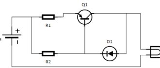
An example of using the AND element in a real technical device: According to technical. According to the task, the mechanical press should operate only when two buttons separated by a certain distance are pressed simultaneously. The meaning of those The task is to ensure that both hands of the operator are occupied while the press is moving, which would eliminate the possibility of accidental injury to a limb. This can be implemented just using the AND gate.
Logic circuit AND - NOT.
NAND is the most commonly used element. It consists of AND and NOT logic gates connected in series.
OR logic circuit.
OR is a logical addition circuit. A logical one at the output appears if a high level (one) is present at any of the inputs.
Logic circuit OR - NOT.
OR - NOT consists of logical elements OR and NOT connected in series. Accordingly, it does NOT invert the values at the OR output.
Exclusive OR logic circuit.
This gate produces a logical one at the output if one of the inputs is one and the other is zero. If the inputs have the same values, the output is zero.
Trigger device
A trigger in its circuit design is very similar to the simplest electronic device - a multivibrator. But unlike him, he has two stable positions. These states are provided by changes in the input signal when it reaches a certain value. The transition from one position to another is called a transfer. As a result, a voltage surge occurs at the output of the logic element, the shape of which depends on the speed of the processes taking place in radio devices.
The most widely used trigger is one that operates on transistors. This is due to the ability of the latter to work in key mode. A bipolar transistor is a semiconductor device that has three terminals. These electrodes are called:
- emitter;
- base;
- collector.
To a rough approximation, a transistor consists of two diodes connected by an electrical connection. It consists of two pn junctions. The name bipolar element is due to the fact that it simultaneously uses two types of charge carriers. In trigger circuits, the transistor operates in switch mode, the essence of which is to control the strength of the collector current by changing the value at the base. In this case, the collector current exceeds the base current in magnitude.
With this connection, only currents are important, and voltages do not play a special role. Therefore, when a certain current occurs at the base, the transistor opens and passes a signal through itself. The signal at the collector of the semiconductor device will have the opposite sign of the input, that is, inverted. This means that when there is a potential difference at the base output, it will be equal to zero at the collector output, and vice versa.
This ability of transistors is used in flip-flops, the circuit of which is built on two switches with cross feedback connections. When transistor switches with the same wiring are used, the trigger is considered symmetrical, in the other case - asymmetrical.
Principle of operation
Stable states of the trigger output are provided by two transistor switches covered by positive feedback (POF). Such positions correspond to the state when one of the transistors is open and in saturation mode, and the second switch is closed. In this case, at the collector of the closed element there is a potential difference equal to its value at the input - a logical one, and at the output of the open key there is no voltage - a logical zero.
Bipolar components with such inclusion relative to each other will always be in the opposite state due to feedback. Through it, one of the transistors (closed) with a high voltage level at its collector terminal will necessarily maintain the other in the open state.
You may be interested in Uninterruptible power supplies (UPS) for computers
If we assume that after power is supplied to the device, both transistors VT1 and VT2 will be open, then after a while, due to the difference in the characteristics of the radio elements located in their shoulders, a imbalance will occur in the collector currents . And this, thanks to the PIC, will lead to the closure of one of the keys. That is, feedback will provoke an avalanche-like process of transition of one transistor to saturation mode, and the other to cutoff mode.
Dividers assembled on resistors R1, R4 and R2, R3 are selected so that their transmission coefficient is less than unity. Moreover, to maintain the signal level, they are shunted with a capacitance, which accelerates the speed of avalanche-like processes and increases the reliability of the state.
Thus, the principle of operation of a trigger is to go through the following processes. If voltages Ek and Eb are applied to the circuit, then bipolar switch VT1 begins to operate in saturation mode, and VT2 in cutoff mode. The pulse arriving at the base of VT1 leads to a decrease in the amount of current flowing through the collector and an increase in the voltage at the collector-emitter junction U1ke. Voltage through C1 and R4 is applied to the base of VT2. This leads to an increase in the collector current on the second switch and a decrease in the voltage at the junction U2ke, transmitted through C2 and R3 to the base of VT1.
The result of these processes will be the locking of VT1 and the unlocking of VT2. This state will remain unchanged until a negative signal level arrives at the VT2 base. The result of this will be reverse electrical processes, and VT1 will close and VT2 will open.
Device characteristics
A trigger can conventionally be called an “automatic machine” capable of storing one bit of information. The simplest type of device has two outputs, which are in an inverse state relative to each other. Important device parameters are related to the synchronization (clocking) of the outputs, which depends on the preset time and dwell time. The first parameter is characterized by the time interval during which the enabling edge of the clock signal arrives, and the second is determined by the time the stable state remains in a constant position. A number of other characteristics of a trigger are associated with the signal passing through it. These include:
- load capacity - characterized by the branching coefficient (Kp) and indicates the ability of the device to control a certain number of elements connected in parallel to the output of the device;
- Ko is the combination coefficient, indicating the largest number of input voltages that can be connected to the input of the device;
- ti is the minimum duration of the input signal, that is, the duration of the pulse at which the trigger can still go into the inverse state;
- tzd - delay coefficient, indicates the time interval between the supply of the input signal and the appearance of voltage at the output;
- tр is the duration of the resolution, determined by the minimum time elapsed between two signal pulses at the input and triggering the transition of the trigger to another state.
You may be interested in Electronic voltage converter from 12 V to 220 V
But along with this, the following technical parameters of triggers are distinguished:
- input voltage - the largest potential difference that the device can withstand without damaging its internal electrical circuit;
- current consumption - depends on the elements used, usually does not exceed 2 mA;
- switching potential difference is the minimum value at which the output is inverted;
- input current - indicates the minimum value required for the trigger to operate;
- output current - the current value that appears at the output and is determined separately for logical zero and one;
- temperature range - the interval in which the technical parameters of the device do not change;
- Hysteresis voltage is the difference in the amplitudes of the input signal, leading to a change in the state of the device’s output.