Linear stabilizers have a common disadvantage - low efficiency and high heat generation. Powerful devices that create load current over a wide range have significant dimensions and weight. To compensate for these shortcomings, pulse stabilizers have been developed and used.
A device that maintains a constant voltage at a current consumer by adjusting an electronic element operating in key mode. A switching voltage stabilizer, just like a linear one, exists in series and parallel types. The role of the key in such models is played by transistors.
Since the effective point of the stabilizing device is almost constantly located in the cutoff or saturation region, passing through the active region, a little heat is generated in the transistor, therefore, the pulse stabilizer has a high efficiency.
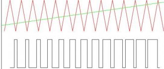
Stabilization is carried out by changing the duration of the pulses, as well as controlling their frequency. As a result, a distinction is made between pulse-frequency and, in other words, width-width regulation. Pulse stabilizers operate in a combined pulse mode.
In stabilization devices with pulse-width control, the pulse frequency has a constant value, and the duration of the pulses is a variable value. In devices with pulse-frequency control, the duration of the pulses does not change, only the frequency is changed.
At the output of the device, the voltage is presented in the form of ripples; accordingly, it is not suitable for powering the consumer. Before supplying power to the consumer load, it must be equalized. To do this, leveling capacitive filters are mounted at the output of pulse stabilizers. They come in multi-link, L-shaped and others.
The average voltage applied to the load is calculated by the formula:
- Ti is the duration of the period.
- ti – pulse duration.
- Rн – value of consumer resistance, Ohm.
- I(t) – value of the current passing through the load, amperes.
Current may stop flowing through the filter by the start of the next pulse, depending on the inductance. In this case we are talking about the operating mode with alternating current. The current can also continue to flow, which means operation with direct current.
With increased sensitivity of the load to power pulses, the DC mode is performed, despite significant losses in the inductor winding and wires. If the size of the pulses at the output of the device is insignificant, then operation with alternating current is recommended.
Principle of operation
In general, a pulse stabilizer includes a pulse converter with an adjustment device, a generator, an equalizing filter that reduces voltage pulses at the output, and a comparing device that supplies a signal of the difference between the input and output voltages.
A diagram of the main parts of the voltage stabilizer is shown in the figure.
The voltage at the output of the device is supplied to a comparing device with the base voltage. The result is a proportional signal. It is supplied to the generator, having previously amplified it.
When controlled in a generator, the difference analog signal is modified into a ripple with a constant frequency and variable duration. With pulse-frequency control, the duration of the pulses has a constant value. It changes the frequency of the generator pulses depending on the properties of the signal.
The control pulses generated by the generator pass to the elements of the converter. The control transistor operates in key mode. By changing the frequency or interval of the generator pulses, it is possible to change the load voltage. The converter modifies the output voltage value depending on the properties of the control pulses. According to theory, in devices with frequency and width adjustment, voltage pulses at the consumer may be absent.
With the relay principle of operation, the signal, which is controlled by the stabilizer, is generated using a trigger. When constant voltage enters the device, the transistor, which acts as a switch, is open and increases the output voltage. the comparing device determines the difference signal, which, having reached a certain upper limit, changes the state of the trigger, and the control transistor switches to cutoff.
The output voltage will begin to decrease. When the voltage drops to the lower limit, the comparing device determines the difference signal, switching the trigger again, and the transistor will again go into saturation. The potential difference across the device load will increase. Consequently, with a relay type of stabilization, the output voltage increases, thereby equalizing it. The trigger limit is adjusted by adjusting the amplitude of the voltage value on the comparing device.
Relay-type stabilizers have an increased response speed, in contrast to devices with frequency and width control. This is their advantage. In theory, with a relay type of stabilization, there will always be pulses at the output of the device. This is their disadvantage.
Pulse (key) voltage stabilizers
The stabilizers discussed above operate in a continuous mode, i.e., the regulating element (transistor), through the action of feedback, continuously changes its internal resistance and at the same time power is continuously released on it, which is the most significant in the overall power balance. Therefore, the efficiency of these stabilizers does not exceed 40-60%.
The efficiency is much higher (up to 90%) for pulsed or key voltage stabilizers (ISN), the regulating element of which is a periodically closed and opened transistor switch (Figure 42,a), and voltage stabilization is achieved by controlling the duration of the pulses supplied to the regulating transistor.
When the duration of the control pulses changes, the duration of the output voltage pulses changes accordingly (Figure 42, b), which determines the change in the average voltage across the load. Thus, if a feedback signal is introduced into the control circuit, proportional to the deviation of the average voltage value at the load from the set value, then the circuit will allow stabilization of the output voltage. Since the output voltage in this case is in the form of pulses, unlike continuous stabilizers, a smoothing filter is required in the ISN.
Figure 42 - Operation of the transistor in switching mode; (a) - transistor switching circuit; b - diagrams of the base current and output voltage in the circuit
Figure 43 — Block diagram of a pulse voltage stabilizer
The block diagram of the ISN is shown in Figure 43. The stabilizer includes a regulating element and a smoothing filter, as well as a control circuit consisting of a comparison circuit, an amplifier and a converter. The comparison circuit and the amplifying element of the circuit are similar to the corresponding elements of continuous compensation stabilizers, and pulse generators, multivibrators, and triggers are used as a converter in these circuits, the pulse parameters of which change depending on the constant signal coming from the amplifier.
Figure 44 – Characteristics of the transistor in switch mode
In the switching mode, the operating point of the transistor for most of the switching period is in two states: saturation (the transistor is open) and cutoff (the transistor is closed), which corresponds to curves 1 and 2 of the characteristics of the transistor in the switching mode (Figure 44). The working sections are the inclined section of curve 1 and a flat section of curve 2; The area between them is called the active region of the transistor.
It is important to note that both in the saturation state and in the cutoff state, the power released in the transistor is small, since either the voltage or current of the transistor is very large, while the active power zone of the transistor operating point passes at high speed only at the moments of switching on, while the value The average (over the switching period) power dissipated by the control transistor is much less than when it operates in continuous mode. Therefore, ISNs have a higher efficiency (up to 95%) and better weight and size characteristics compared to stabilizers with continuous voltage regulation.
According to the method of switching on the control transistor and the inductor, the ISN can be divided into serial and parallel. Let's consider options for connecting the elements of the power part of the ISN.
If a direct current source is connected to a load using a periodically closed and opened switch (transistor), then the average voltage value of the load will be
,
where tI is the duration of the pulse in the closed state of the key; T is the switching period; i(t)—current current value. If the switch load is inductive (when this load is shunted with a diode), such a device can be considered as a DC autotransformer. If you connect a capacitor of sufficiently large capacity in parallel with the load, then the alternating component of the circuit current will be closed through it, and the voltage ripple across the load will be insignificant. This condition can be met with three options for connecting power elements, presented in Figure 45. Let us explain the features of the circuits.
A circuit with a sequential connection of a transistor and an inductor (Figure 45, a) allows you to obtain a voltage under load that is equal to or less than the supply voltage. A circuit with a serial connection of a transistor and a parallel connection of a choke (Figure 45b) allows you to obtain a voltage greater or less than the supply voltage, while the voltage at the output of the stabilizer is inverted.
Figure 45 — Connection diagrams of power elements in pulse stabilizers and the dependence of UН / UП on the pulse fill factor for these circuits
A circuit with a parallel connection of a transistor and a series connection of a choke (Figure 45, c) allows you to obtain a voltage equal to or greater than the supply voltage.
Figure 45d shows the dependences of the load voltage for the three indicated circuits on the duty cycle of the pulses Кз = tИ /T, where tИ/T is the relative pulse duration. It should be noted that the load voltage in this case is also given in relative units UN/UP, the latter ratio is defined as the DC voltage transfer coefficient from the circuit input to the load. In conclusion, it should be noted that various options for constructing power circuits of transistor ISNs are known, but all of them can be reduced to the three discussed above.
Based on the control method, switching stabilizers are divided into stabilizers with pulse-width modulation (PWM), with pulse-frequency modulation (PFM) and relay or on-off stabilizers.
Stabilizers with PWM and PFM
In stabilizers with PWM, a generator is used as a pulse element, the pulse or pause time of which varies depending on the constant signal arriving at the input of the pulse element from the output of the comparison circuit.
The principle of operation of a PWM stabilizer is as follows: a constant voltage from a rectifier or battery is supplied to a regulating transistor, and then through a filter to the output of the stabilizer, the output voltage of the stabilizer is brought to the reference voltage, compared with it, and then the difference signal is applied to the input of the device, converting a direct current signal into pulses of a certain duration, the latter changing in proportion to the difference signal between the reference and measured voltage. From a device that converts direct current into pulses, the signal is sent to a control transistor; the latter periodically switches and the average voltage value at the filter output depends on the ratio between the time the transistor is in the open and closed states (on the pulse width - hence the name of this type of modulation), and the PWM pulse repetition rate is constant. When the voltage at the output of the stabilizer changes, the direct current signal changes, and therefore the width (duration) of the pulse (at a constant period); As a result, the average value of the output voltage returns to its original value.
In stabilizers with PWM, when the signal at the output of the pulse element changes, the duration of the pause changes, and the duration of the pulse remains unchanged, and, unlike stabilizers with PWM, in these stabilizers the switching frequency of the control transistor depends on changes in the load current and output voltage, and therefore is a changing, non-constant value - hence the name of this type of modulation. The operating principle of such stabilizers is similar to the operating principle of PWM stabilizers. A change in the output voltage of the stabilizer causes a change in the pause, which leads to a change in the pulse frequency and the average value of the output voltage remains unchanged.
The operating principle of relay or on-off stabilizers is somewhat different from the operating principle of PWM stabilizers. In relay stabilizers, a trigger is used as a pulse element, which in turn controls a regulating transistor. When a constant voltage is applied to the input of the stabilizer, at the first moment the regulating transistor is open and the voltage at the output of the stabilizer increases, and the signal at the output of the comparison circuit increases accordingly. At a certain value of the output voltage, the signal at the output of the comparison circuit reaches a value at which the trigger is triggered, closing the control transistor. The voltage at the output of the stabilizer begins to decrease, which causes a decrease in the signal at the output of the comparison circuit. At a certain signal value at the output of the comparison circuit, the trigger fires again, opens the control transistor and the voltage at the output of the stabilizer begins to increase; it will increase until the trigger closes the control transistor again, and thus the process repeats.
A change in the input voltage or load current of the stabilizer will lead to a change in the open state time of the control transistor and to a change in its switching frequency, and the average value of the output voltage will be maintained (with a certain degree of accuracy) unchanged. Thus, as in PFM stabilizers, in relay stabilizers the switching frequency of the control transistor is not constant.
In conclusion, it is necessary to note the advantages and disadvantages of the described stabilizers. In principle, output voltage ripple in stabilizers with PWM and PWM may be completely absent, since the pulse element is controlled by the constant component of the control circuit signal; In relay stabilizers, output voltage pulsations must fundamentally take place, since periodic switching of the trigger is possible only when the output voltage periodically changes. One of the main disadvantages of PWM and PWM stabilizers compared to relay ones is their lower operating speed.
Let's look at the circuits and operation of a relay stabilizer and a PWM stabilizer.
Figure 46 — Diagram of a pulse relay voltage stabilizer (a) and graphs of voltages and currents in it (b)
Figure 46, a shows the circuit of a relay voltage stabilizer, which consists of a composite control transistor (VT11, VT12); filter (L, CH, VD2); comparison and DC amplifier (R1 RP, R2, VDOP, RG, VTU); trigger on a tunnel diode VDTG, transistor VT4 and resistor R8; intermediate amplifier VT3, R5, R4, R3); transistor VT2, designed to turn off the control transistor; chain R9, C1, necessary to increase the frequency of self-oscillations of the stabilizer, as well as elements R6, RZAP, VD1 SZAP, necessary for reliable opening and closing of the control transistor.
In this circuit, a trigger based on a tunnel diode and a transistor is used as a pulse element. In such circuits, you can use a trigger on transistors (Schmitt trigger), but the use of a trigger on a tunnel diode allows you to improve the fronts of control pulses and reduce the number of elements.
The operating principle of the circuit is as follows. A constant voltage UВХ is supplied to the input of the stabilizer. At time t0, the voltage at the output of the stabilizer decreases to a value corresponding to the activation of the trigger VT4 VDTG. The trigger is triggered, and the VT4 collector current abruptly decreases to zero. In this case, transistors VT3 and VT2 close; transistors VT12, VT11 open, and the capacitor SZAP is charged through resistor R6. The voltage at the filter input (at points A, B) increases abruptly to voltage UBХ, diode VD2 closes and the current flowing through it drops to zero. The collector current of the regulating transistor VT11, and accordingly the inductor current, begins to increase, and the voltage at the output of the stabilizer begins to decrease, and it decreases until the current flowing through the inductor becomes equal to the load current IN; then the tension begins to rise. As the output voltage increases, the positive potential at the base of the transistor VTy increases, while the base current, and therefore the collector current VTy, increases.
At time t1, the voltage at the output of the stabilizer becomes equal to UBИХ+ UТГ/ (see Figure 46, b), and the collector current VTy reaches the value of the trigger current. The trigger is triggered, and the collector current VT4 jumps to the maximum value. Transistors VT3 and VT2 open. The SZAP capacitor is connected through transistor VT2 between the base and emitter of transistors VT12, VT11 and they close. In the interval t1 – t2, the collector current of the transistor VT11 iK11 is zero, and the inductor is discharged through the diode VD2. The voltage at the output of the stabilizer first increases (while the current in the inductor L is greater than the load current), and then begins to decrease.
As the output voltage decreases, the positive voltage at the base of the transistor VTy decreases and its base and collector currents decrease. At time t2, the voltage UOUTH- at the output decreased to the value UOUTH- UТГ/, and the collector current VTy decreased to the value of the trigger release current. The trigger is triggered, transistors VT4, VT3, VT2 close, and transistors VT12, VT11 open. The collector current of the regulating transistor VT11 begins to increase again, and accordingly the inductor current L. Thus, the process is continuously repeated.
When the input voltage or load current changes, the duty cycle of the control transistor pulses changes, and the average value of the output voltage remains unchanged with a certain degree of accuracy. As can be seen from the principle of operation of the circuit, stabilizers of this type operate in the mode of stable self-oscillations.
As mentioned above, relay stabilizers are, in principle, inherent in output voltage pulsations, but it should be noted that the relatively large amplitude of these ripples, being the main disadvantage of other stabilizers, limits their scope of application. The amplitude of the output voltage ripple depends on the trigger thresholds, the gain of the amplifier and on the value of the attenuation coefficient of the stabilizer filter, and with a decrease in the trigger thresholds and an increase in these coefficients, the ripple amplitude decreases. However, even with zero trigger thresholds, an infinite amplifier gain and a sufficiently large filter attenuation coefficient (and at large values of the latter, the overall dimensions of the stabilizer sharply increase), it is not possible to obtain a small pulsation amplitude. A significant reduction in the ripple amplitude is achieved by increasing the frequency of self-oscillations of the stabilizer with the same parameters of the filter, amplifier and trigger.
Boost stabilizer
Switching boost regulators are used with loads whose potential difference is higher than the voltage at the input of the devices. The stabilizer does not have galvanic isolation between the power supply and the load. Imported boost stabilizers are called boost converters. The main parts of such a device:
The transistor enters saturation, and current flows through the circuit from the positive pole through the storage inductor, the transistor. In this case, energy accumulates in the magnetic field of the inductor. The load current can only be created by a discharge of capacitance C1.
Let's turn off the switching voltage from the transistor. At the same time, it will enter the cut-off position, and therefore a self-induction EMF will appear on the throttle. It will be switched in series with the input voltage, and connected via a diode to the consumer. The current will flow through the circuit from the positive pole to the inductor, through the diode and the load.
At this moment, the magnetic field of the inductive choke supplies energy, and capacitance C1 reserves energy to maintain the voltage at the consumer after the transistor enters saturation mode. The choke is for energy reserve and does not work in the power filter. When voltage is applied again to the transistor, it will open and the whole process will begin again.
Switching DC voltage stabilizers
In compensating stabilizers with continuous regulation, the efficiency is usually directly proportional to the ratio and therefore is relatively small, i.e. 50-60%. Switching voltage stabilizers (SVS) allow you to obtain greater output power () and efficiency. In the ISN, the regulatory element, i.e. the transistor operates in switching mode. This is their main difference from continuous stabilizers. When operating in switch mode, the operating point of the transistor is either in the saturation region or in the cutoff region. And in the active region zone, the operating point arrives at high speed and only at the moment of switching. The voltage in the cutoff state in the saturation state the power dissipated by the transistor is small, because respectively small (0.3) and . The total power dissipated by the transistor also includes switching losses at the moment of switching from cutoff to saturation and back. It should be noted that the power dissipated by the control transistor in pulsed mode is much less than when it operates in continuous mode. Therefore, ANNs, compared to continuous stabilizers, have a higher efficiency and can improve weight and size parameters. By reducing the size of the transformer and cooling radiators for the control transistor. The disadvantages of INS include: a more complex control scheme, increased noise and ripple levels, as well as worse dynamic characteristics. The generalized ANN diagram looks like this.
Dr-throttle.
SU - control circuit.
F - inductive-capacitive smoothing filter.
The principle of operation of the ISN is to convert, using RE, a constant voltage into a sequence of periodic unipolar rectangular pulses. The control system, using the OOS circuit, influences the timing parameters of the pulses, i.e. on their duration and frequency. So that the average value remains constant.
The filter serves to convert semi-scientific pulses into direct voltage. When T is open and saturated and the inductor current is equal to the transistor current. At the same time, energy accumulates in the throttle. When T is locked in the throttle, a self-induction emf is induced. As a result, diode D opens. Depending on the method of stabilization, ISN are divided into three groups:
ISN with PWM (pulse wide modulation);
ISN with PFM (pulse frequency modulation);
ISN with RSR (relay control system).
ISN with PWM. The duration of the pulses at the filter input is inversely proportional to the value. In this case, the pulse frequency is constant.
ISN with FIM. The duration of the pulses is constant, and the intervals between them are proportional. The pulse frequency is inversely proportional.
ISN with RSR. The formation of pulses occurs at the moment of intersection of two horizontal levels: the lower one when the front is formed and the upper one when the cut is formed (the end of the pulse). Depending on the frequency and duration may vary widely. The formation of pulses can be a Schmitt trigger, which has two types of triggering.
ISN with BUS has the following advantages compared to other types of ISN:
1) high efficiency and optimal frequency are ensured, regardless of and. This means that the pulsation frequency is constant and has significant values
2) a real possibility of simultaneous synchronization of conversion frequencies of an unlimited number of ISNs. This eliminates the risk of frequency beats when several ISNs are powered from a common one.
The disadvantage of an ISN with PWM, in contrast to a relay-type ISN, is a more complex control system, usually containing an additional master oscillator.
ISN with PFM, while not having significant advantages over other types of ISN, has the following disadvantage: the complexity of the circuitry of frequency control over a wide range, especially with large changes in and.
ISN with RCP has the advantage of a simple control circuit.
ISN control circuit with PWM
Various devices are used as a control circuit (CS), giving preference to those that are implemented on digital technology elements. Here, the most widely used method is based on comparison with sawtooth voltage. Let's draw a diagram that implements this method.
K-comparator.
CC - comparison scheme.
GPN is an antiderivative voltage generator.
In the SS performed on an operational amplifier, the stabilizer is compared with that obtained under the ION. The analog error signal from the CC pin is fed to one of the inputs of the comparator, the other input of which is supplied with a sawtooth voltage under the GPG. During the time the analog error signal exceeds the sawtooth voltage, a pulse PWM is generated.
From Fig. It can be seen that the repetition rate of the PWM pulses is set by a sawtooth voltage, and their duration is set by the level of the error signal.
Currently, almost the entire control circuit can be implemented in one crystal, like a large microcircuit. It consists of: a circuit with PWM, ION, a protection circuit, and a pulse generation circuit for the control transistor. For example, MS K142 EP1 consists of 5 functional units: ION, OS signal amplifier, PWM circuit, control pulse amplifier, micro-power power transistors. At low load currents up to 50 MS, it can be used as a complete voltage stabilizer. At high currents, the MS can be used as a circuit for controlling powerful transistors with ISN switches.
ISN with RSR
In such ISNs, the frequency and duration of control pulses of the regulating transistor can change within wide limits depending on.
The circuit works as follows: transistor T can be in either a saturation state or a cutoff state. Upon arrival, T is open and saturated, the current through the inductor Dr charges the capacitor C. In this case, the voltage on the capacitor C, equal to , increases until it exceeds the inverting input of the op-amp. At this moment, the op-amp stops powering the T base, which is locked. The energy stored in the inductor causes a current to flow through the load and diode D. Capacitor C discharges and decreases. When the voltage at the inverting input becomes less, the op-amp turns on the transistor switch again and the cycle repeats. fluctuates around = . The amplitude of the oscillations is determined by the gain of the op-amp and the ratio For the considered relay-type stabilizer circuit, we can assume that the operating voltage is equal to the release voltage, i.e. the formation of impulses occurs at the moments of intersection of not two, but one horizontal level equal to .
Switching stabilizers with pulse width modulation and relay stabilizers
The operation of the transistor in switching mode is characterized by a rapid transition of the operating point from the cutoff region to the saturation region. In this case, the power dissipated by the control transistor is many times less than when it operates in linear mode. The operation of the control transistor in switching mode allows you to increase the utilization rate of the transistor itself, increase the efficiency of the stabilizer and reduce its dimensions. The most common two types of pulse stabilizers are stabilizers with pulse-width modulation and relay stabilizers or stabilizers with on-off regulation (Fig. 5.25).
In stabilizers with pulse-width modulation, a generator is used as a pulse element, the duration of the pulse or pause of which varies depending on the constant signal arriving at the input of the pulse element from the output of the comparison circuit. The principle of operation of a stabilizer with pulse-width modulation is as follows: a constant voltage U0 from a rectifier or from a battery is supplied to a control transistor, and then through a filter to the output of the stabilizer. The output voltage of the stabilizer is brought to the reference voltage, compared with it, and then the difference signal is applied to the input of a device that converts the direct current signal into pulses of a certain duration. The duration of the pulses changes in proportion to the difference signal between the reference and measured voltages. From a device that converts direct current into pulses, the signal is sent to a regulating transistor.
The regulating transistor switches periodically, and the average voltage value at the filter output depends on the duty cycle of the pulses. When the voltage at the output of the stabilizer changes, the DC signal changes, and, consequently, the duty cycle of the control transistor pulses, and the average value of the output voltage returns to its original value.
The principle of operation of relay or two-position stabilizers is somewhat different from the principle of operation of stabilizers with pulse width modulation. In relay stabilizers, a trigger is used as a pulse element, which, in turn, controls a regulating transistor. When a constant voltage is applied to the input of the stabilizer, at the first moment, the control transistor is open, and the voltage at the output of the stabilizer increases. Accordingly, the signal at the output of the comparison circuit increases. At a certain value of the output voltage, the magnitude of the signal at the output of the comparison circuit will become sufficient to trigger the trigger. The trigger fires and closes the control transistor. The voltage at the output of the stabilizer begins to decrease, which causes a decrease in the signal at the output of the comparison circuit. At a certain signal value at the output of the comparison circuit, the trigger is triggered again and opens the control transistor. The voltage at the output of the stabilizer begins to increase. The output voltage will increase until the trigger closes the control transistor again. Thus, the process will be repeated. A change in the input voltage or load current of the stabilizer will lead to a change in the duty cycle of the control transistor pulses and a change in its switching frequency, and the average value of the output voltage will be maintained unchanged with a certain degree of accuracy.
Stabilizers of the first and second types differ in the following.
In stabilizers of the first type, the switching frequency of the control transistor is constant; in stabilizers of the second type, the frequency depends on changes in the load current and input voltage. The output voltage ripple in stabilizers of the first type can in principle be equal to zero, since the pulse element is controlled by the constant component of the comparison circuit signal.
The ripple at the output of stabilizers of the second type cannot in principle be equal to zero, since periodic switching of the trigger is possible only with periodic changes in the output voltage.
One of the main disadvantages of stabilizers of the first type is their low speed. When such stabilizers are powered from a rectifier, the input voltage ripple is reduced slightly by the stabilizer, and therefore its filter must rely on the low-frequency component of the ripple.
The disadvantage of stabilizers of the second type is the dependence of the switching frequency on changes in the network voltage and load current. It should be noted that this drawback can be eliminated in relay stabilizers. To do this, an alternating signal is supplied from an external generator to the input of the amplifier or the trigger itself. If the amplitude of the alternating signal exceeds the trigger thresholds, then under certain conditions the stabilizer is synchronized and it operates in pulse-width modulation mode.
In this case, when the input voltage or load current changes, the frequency remains unchanged, but the duty cycle of the control transistor pulses changes.
In Fig. 5.26, 5.27 show circuits of relay voltage stabilizers. The main difference between the schemes is the different operating modes. Stabilizer fig. 5.26 works in normal mode, and the stabilizer Fig. 5.27 operates in pulse width modulation mode. Let's take a closer look at the operation of these circuits. Stabilizer fig. 5.26 consists of a composite control transistor (T11, T12); filter (L1, Сн, D2); constant volume comparison and amplifier circuits (R1, Rн, R2, D1, Rг1, Tu, Ru); trigger on tunnel diode D3 and transistor T4, intermediate amplifier (T3, R3, R3); transistor T2, designed to turn off the control transistor; chain R9, C1, necessary to increase the frequency of self-oscillations of the stabilizer and elements R6, RZAP, D4 SZAP, necessary for reliable switching on and overwriting of the control transistor.
In this circuit, a trigger based on a tunnel diode and transistor is used as a pulse element. As shown in, in such circuits you can use a trigger on transistors (Schmitt trigger), however, the use of a trigger on a tunnel diode allows you to improve the fronts of control pulses and reduce the number of elements.
In Fig. Figure 5.28 shows graphs of the output voltage of the stabilizer, currents and voltages of transistor T11 and diode D2 and current in inductor Dr1.
Let's consider the principle of operation of the circuit in Fig. 5.26. A constant voltage U0 is supplied to the input of the stabilizer. At time t = 0, the voltage at the output of the stabilizer decreases to the trigger value (T4D3). The trigger fires, and the collector current T4 abruptly decreases to zero. In this case, transistors T3 and T2 close, transistors T12, T11 open, and the capacitance of the SZAP is charged through resistance R6. The voltage at the filter input (at points A, B) increases abruptly to voltage U0, diode D2 closes, and current ID2 drops to zero. The collector current of the regulating transistor T11, and accordingly the inductor current, begins to increase. The voltage at the output of the stabilizer decreases until the current in the inductor becomes equal to the load current In, and then begins to increase. As the output voltage increases, the positive potential at the base of the transistor Tu increases. The base current, and therefore the collector current Tu, increases.
At time t1, the voltage at the output of the stabilizer reaches the value Uout+∆Utr/α, and the collector current Tу reaches the value of the trigger current. The trigger is triggered, and the collector current T4 jumps to the maximum value.
Transistors T3 and T2 open. The SZAP capacitance is connected through transistor T2 between the base and emitter of transistors T12, T11 and they close. In the interval t1-t2, the collector current of transistor T11 is zero, and the inductor is discharged through diode D2. The voltage at the output of the stabilizer first increases while the current in the inductor D p1 is greater than the load current, and then begins to decrease.
As the output voltage decreases, the positive voltage at the base of the transistor Tu decreases and its base and collector currents decrease. At moment t2, the output voltage decreased to the value Uout-∆Utr/α, and the collector current Tu decreased to the value of the trigger release current. The trigger fires, transistors T4, T3, T2 close, and transistors T12, T11 open. The collector current of the regulating transistor T11 begins to increase again, and accordingly the inductor current Dr1. Thus, the process is continuously repeated.
When the input voltage or load current changes, the duty cycle of the control transistor pulses changes, and the average value Uout of the output voltage remains unchanged with a certain degree of accuracy.
As can be seen from the principle of operation of the circuit, stabilizers of this type operate in the mode of stable self-oscillations.
The main disadvantage that limits the scope of application of relay stabilizers is the relatively large amplitude of the output voltage ripple. The amplitude of the output voltage ripple depends on the magnitude of the trigger thresholds, the gain of the amplifier and the attenuation coefficient of the stabilizer filter. An increase in the resonant frequency of the filter at constant levels of trigger thresholds, constant values of the amplifier gain and the attenuation coefficient of the stabilizer filter causes a proportional increase in the frequency of self-oscillations without changing the magnitude of the output voltage ripple.
The attenuation coefficient of the filter increases by increasing the inductance of the inductor, with a corresponding decrease in the filter capacitance (from the condition of the constant resonant frequency of the filter). At large values of the attenuation coefficient, the dimensions of the stabilizer increase sharply. However, even with zero trigger thresholds, an infinite amplifier gain and a sufficiently large attenuation coefficient, it is not possible to obtain a small pulsation amplitude.
As is known from the theory of relay automatic control systems, an increase in the frequency of self-oscillations with constant filter parameters, fixed trigger thresholds and a constant amplifier gain can be achieved by introducing additional accelerating elements. As such an accelerating element in this circuit, a chain consisting of capacitance C1 and resistance R9 is used. A significant increase in the frequency of self-oscillations of the stabilizer with the same parameters of the filter, amplifier and trigger leads to a significant decrease in the ripple amplitude.
Stabilizer diagram Fig. 5.27 in terms of the composition of elements is not much different from the diagram in Fig. 5.26. The main difference is that instead of resistance RZAP, diodes D5 are installed in the circuit. The use of diodes in the blocking circuit makes it possible to limit the voltage on the capacitance of the SZAP. In addition, when the input voltage changes, the voltage amplitude across the SZAP capacitance changes slightly. The constancy of the amplitude of the blocking voltage is especially important if high-frequency transistors are used as control transistors, in which the base-emitter reverse voltage is small and strictly limited in value.
Unlike the diagram in Fig. 5.26, this stabilizer operates in pulse width modulation mode. An alternating signal is supplied to the amplifier input through an isolation capacitor from an external source. The waveform can be sawtooth or sine wave.
Let's consider the principle of operation of the circuit in Fig. 5.27 under sawtooth alternating influence. In Fig. Figure 5.29 shows graphs explaining the operation of the relay stabilizer in pulse-width modulation mode. An external sawtooth signal and a constant bias Ucm1 from the divider R1, Rп, R2 are supplied to the base of the amplifying transistor. At moment t1, the voltage at the base of the amplifying transistor reaches a value at which the collector current Tу is equal to the trigger current. The trigger is triggered, transistors T4, T3, T2 open, and T12, T11 close. The voltage at the input of the UAB filter abruptly decreases to zero. At time t2, the sawtooth voltage at the base of the transistor Tu decreased to a value at which the collector current of the amplifying transistor became equal to the release current of the trigger. The trigger fires, transistors T4, T3, T2 close, and T12, T11 open. The voltage at the filter input again increases abruptly to the value of the input voltage U01. Thus, the trigger, and accordingly the control transistor, is continuously switched due to an external alternating signal.
Suppose the voltage at the stabilizer input has increased to the value U02. In this case, the bias voltage at the base of the amplifying transistor increased to a value of Ucm2. As can be seen from the graphs in Fig. 5.29, increasing the bias increases the open time of transistors T4, T3, T2. The open time of transistor T12, T11 decreases. Accordingly, the pulse duration at the filter input decreases, and the average value of the output voltage returns to the original value with a certain degree of accuracy.
Previous8Next
Live by the rule: IS THERE NOT MUCH THING IN THE WORLD EXISTING? It is no coincidence that I emphasize that the space in your head is limited, but there is a lot of information around, and that your right...
What Causes Trends in Stock and Commodity Markets Freight Train Theory Explained My first 17 years of market research consisted of trying to figure out when...
What makes your dreams come true? One hundred percent, unshakable confidence in your...
System of Protected Areas in the USA The study of specially protected natural areas (SPNA) in the USA is of particular interest for many reasons...
Didn't find what you were looking for? Use Google search on the site:
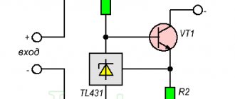
Stabilizers with Schmitt trigger
This type of pulse device has its own characteristics with the smallest set of components. The trigger plays a major role in the design. It includes a comparator. The main task of the comparator is to compare the value of the output potential difference with the highest permissible value.
The principle of operation of the device with a Schmitt trigger is that when the highest voltage increases, the trigger is switched to the zero position with the electronic key opening. At one time the throttle discharges. When the voltage reaches its lowest value, switching by one is performed. This ensures the switch closes and current flows to the integrator.
Such devices are distinguished by their simplified circuit, but they can be used in special cases, since pulse stabilizers are only step-up and step-down.
Buck stabilizer
Pulse-type stabilizers, operating with voltage reduction, are compact and powerful electric power supply devices. At the same time, they have low sensitivity to consumer interference with a constant voltage of the same value. There is no galvanic isolation of the output and input in step-down devices. Imported devices are called chopper. The output power in such devices is always less than the input voltage. The circuit of a buck-type pulse stabilizer is shown in the figure.
Let's connect the voltage to control the source and gate of the transistor, which will enter the saturation position. It will carry current through the circuit from the positive pole through the equalizing choke and the load. No current flows through the diode in the forward direction.
Let's turn off the control voltage, which turns off the key transistor. After this, it will be in the cut-off position. The inductive emf of the equalizing choke will block the path for changing the current, which will flow through the circuit through the load from the choke, along the common conductor, diode, and again come to the choke. Capacitance C1 will discharge and will maintain the voltage at the output.
When an unlocking potential difference is applied between the source and gate of the transistor, it will go into saturation mode and the entire chain will repeat again.
What is a step-down switching voltage stabilizer?
Devices of this type are powerful and compact power devices. They have low sensitivity to consumer interference and a constant voltage of the same value. At the same time, galvanic isolation of the input and output is practically absent. The output power of such devices is always less than the input voltage.
It is quite simple to assemble a pulse voltage stabilizer of this type with your own hands. In short, the circuit diagram looks like this: a voltage is connected, which is used to control the source and gate of the transistor. It should go to saturation position. Current flows from the positive pole to the equalizing choke and the load. It does not flow in the forward direction. When the control voltage is turned off, the key transistor turns off. After this, it remains in the cut-off position. The electromotive force of induction of the equalizing choke blocks the path for the change in current flowing through the circuit. At the same time, it passes through the load, goes along the common conductor and returns to the inductor. As a result, the voltage level decreases.
Inverting stabilizer
Inverting-type switching stabilizers are used to connect consumers with constant voltage, the polarity of which has the opposite polarity direction to the potential difference at the output of the device. Its value can be above the power supply network, and below the network, depending on the settings of the stabilizer. There is no galvanic isolation between the power supply and the load. Imported inverting type devices are called buck-boost converters. The output voltage of such devices is always lower.
Let's connect a control potential difference, which will open the transistor between the source and the gate. It will open, and the current will flow through the circuit from the plus through the transistor, the inductor, to the minus. In this process, the inductor reserves energy using its magnetic field. Let's turn off the control potential difference from the switch on the transistor, it will close. The current will flow from the inductor through the load, diode, and return to its original position. The reserve energy on the capacitor and magnetic field will be consumed by the load. Let's apply power to the transistor again to the source and gate. The transistor will again become saturated and the process will repeat.
Advantages and disadvantages
Like all devices, a modular switching stabilizer is not ideal. Therefore, it has its own pros and cons. Let's look at the main advantages:
- Easily achieve alignment.
- Smooth connection.
- Compact sizes.
- Output voltage stability.
- Wide stabilization interval.
- Increased efficiency.
Disadvantages of the device:
- Complex design.
- There are many specific components that reduce the reliability of the device.
- The need to use power compensating devices.
- Difficulty of repair work.
- Formation of a large amount of frequency interference.
Allowable frequency
The operation of a pulse stabilizer is possible at a significant conversion frequency. This is the main distinguishing feature from devices that have a network transformer. Increasing this parameter makes it possible to obtain the smallest dimensions.
For most devices, the frequency range will be 20-80 kilohertz. But when choosing PWM and key devices, it is necessary to take into account high current harmonics. The upper limit of the parameter is limited by certain requirements that apply to radio frequency devices.
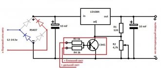
Simple switching voltage stabilizer
Switching voltage stabilizer, circuit
Switching voltage stabilizers have recently become quite popular due to their compact size and relatively high efficiency, and in the near future they will completely replace the good old analog circuits. Now for a couple of dollars in China you can buy a ready-made DC-DC converter module that provides output voltage regulation, has the ability to limit current and operates in a fairly wide range of input voltages.
The most popular chip on which such stabilizers are built is LM2596. Maximum voltage up to 35 volts, with current up to 3 amperes. The microcircuit operates in pulse mode, the heating on it is not very strong under fairly impressive loads, it is compact and costs a penny.
By adding an op-amp, you can also limit the output current; I will say more - current stabilization, in other words - the current will be kept at the set level regardless of the voltage. Such modules are quite compact and can be built into any home-made power supply and charger design. By connecting a digital voltmeter to the output, we will know what voltage is at the output. .
The board itself has trimming resistors to limit the output current and regulate the voltage. The input voltage range will allow such a module to be installed in a car by directly connecting it to the 12 Volt on-board network. What will this give us?
1) Universal charger with high current. You can charge any smartphones, tablets, players and other players, navigators and portable security systems, and you can connect say 2-3 smartphones to the device at the same time and they will all charge equally well.
2) Connect the device, say, to a laptop adapter, set the output to 14-15 Volts and feel free to charge the battery! 3 amperes is quite a considerable current for charging a car battery, although the converter board itself will have to be installed on a small radiator.
You definitely can’t argue with the usefulness of the board, and it costs a penny (no more than 2-3 US dollars). The same board can be made at home, if certain components are available, although the finished module costs much less than individual components.
Dual operational amplifier, the current limiting unit is built on the first oh element, and the indication is built on the second. The microcircuit itself has a harness, a power choke that can be wound independently, and a pair of regulators. The circuit almost does not overheat at low currents - but a small heat sink will not hurt.
Author; AKA Kasyan
← Previous post
Next entry →