The operation of some electrical equipment is impossible without controlling the direction of movement of the electric current. In electronics, a semiconductor diode is effectively used to achieve this goal. The use of a two-terminal network allows you to convert alternating current and direct current into pulsating unidirectional current.
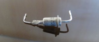
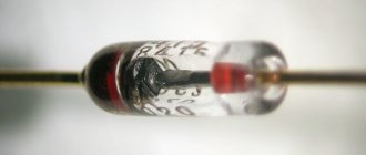
Appearance of a semiconductor diode
Device
A semiconductor diode is a two-terminal device made from a semiconductor substance that allows current to pass in one direction and virtually no current in the other.
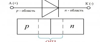
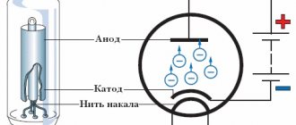
The main element of the diode is a crystalline component with a pn junction, to which a metal anode and a cathode are soldered (welded). The passage of direct current is carried out when a positive potential, relative to the cathode, is applied to the anode.
Note! Holes move in the direction of forward current. The electrons move in the opposite direction.
The diode design can be point, planar, or polycrystalline.
Device of a point and planar p/p device
Additional Information. There are no fundamental differences between point and planar bipolar devices.
The structure of a point diode is shown in figure (a).
When a thin needle, with an impurity deposited on it, is welded to a semiconductor plate with a certain type of electrical conductivity, a hemispherical mini pn junction with a different type of conductivity is formed. This action is called diode forming.
The production of a planar two-terminal network is carried out by the diffusion fusion method. Figure (b) shows an alloy germanium diode and the principle of its design. In a plate of n-type germanium, when a drop of indium is fused there at 500 degrees, a layer of p-type germanium is formed. The lead contacts soldered to the germanium and indium base plate are made of nickel.
Germanium, silicon, gallium arsenide and carbide are used in the production of semiconductor wafers. Semiconductor monocrystalline wafers with a correct structure throughout the entire volume are used as the basis for point and planar two-terminal networks.
In polycrystalline two-terminal networks, the pn junction is formed by semiconductor layers, which include a large number of randomly oriented small crystals that do not represent a single single-crystalline form. These are selenium, titanium and copper oxide bipolars.
Semiconductor diode - device
There are also point (high-frequency) diodes, the area of their p–n junction is less than 0.1 mm2. Such diodes are made by connecting a metal needle to a semiconductor. Point diodes are used in microwave equipment at a current value of 10-20 mA. The main types of semiconductor diodes by functional purpose: rectifiers, zener diodes, pulse diodes, LEDs, photodiodes, etc. Rectifier diodes are semiconductor diodes designed to convert alternating current into direct current.
It will be interesting➡ Diode 1n4007: characteristics, markings and datasheets
Such diodes are made by alloying and diffusion methods in order to create a large pn junction area, since large currents flow through them. The process of rectifying alternating current itself lies in the property of the diode to conduct current well in one direction and practically not conduct it in the other. Below is a diagram of a simple half-wave rectifier. It works as follows: the positive half-cycle of the voltage Uin, the diode V transmits practically without change, and the voltage Ur is almost equal to Uin. But at a time when the half-cycle of the voltage is negative, the diode is turned on in the opposite direction and the entire voltage Uin drops across the diode, and the voltage across the resistor is practically zero.
Semiconductor diodes.
Main characteristics and parameters of diodes
What is a diode - operating principle and device
For the device to work correctly, it must be selected in accordance with:
- Current-voltage characteristic;
- Maximum permissible constant reverse voltage;
- Maximum permissible pulse reverse voltage;
- Maximum permissible direct direct current;
- Maximum permissible pulsed direct current;
- Rated direct direct current;
- Direct direct voltage at rated current;
- Constant reverse current, indicated at the maximum permissible reverse voltage;
- Operating frequency range;
- Capacity;
- Breakdown voltage (for protective diodes and zener diodes);
- Thermal resistance of the housing for various installation options;
- Maximum permissible power dissipation.
Designs and simplest methods for manufacturing semiconductor diodes
To obtain the simplest point diode, they take a metal plate with a lead attached to it and weld a semiconductor crystal of electronic conductivity type to it. This crystal is called the base of the diode. Then they take a metal needle with a lead attached to it, made, for example, of tungsten, gold, beryllium bronze, on which an alloying material is applied, and its sharp tip is pressed against the crystal of the diode base so that the needle is spring-loaded. Aluminum and indium are often used as alloying materials. All parts of the future diode are placed in a housing, which, for example, can be a small glass bottle from which the air is evacuated.
Next, molding is carried out, that is, local heating of the area between the needle and the semiconductor wafer so that their materials diffuse into each other over a small area. To do this, short pulses with a current of about 1 A are passed through the diode in the forward and reverse directions, which is many times higher than the maximum direct current of the point diode being manufactured. The acceptor impurity material that was on the needle and the one from which it consisted diffuse into a small, almost hemispherical area into the base of the diode, forming a junction. Point diodes, due to the small area of the electron-hole junction, usually have a low capacitance, and, therefore, can operate at high frequencies without losing the property of one-way conductivity. However, the small junction area does not allow large forward currents to pass through a point diode without destroying the component.
Semiconductor diode.
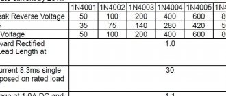
To make a planar diode, they take the base of an electronic diode and place a semiconductor wafer on it, which will later play the role of an acceptor impurity. They are then heated to approximately 450 °C ... 550 °C in a vacuum, causing the acceptor impurity material to diffuse into the base of the future diode. The resulting electron-hole junction will have a large area and significant capacity. The main characteristics of semiconductor diodes are listed in the table below.
Table of main characteristics of semiconductor diodes
Due to the large area of a planar diode, a very large current can be passed through it in direct connection, but the highest frequency at which such a diode can remain operational will be low. In conclusion, it should be noted that there are many other designs, as well as methods for making diodes.
Some basic parameters of semiconductor diodes
The main parameters of diodes include:
- maximum permissible direct direct current, A;
- maximum permissible pulse forward current, A;
- maximum permissible constant reverse voltage, V;
- maximum permissible pulse reverse voltage, V;
- reverse current flowing through the diode in reverse connection when the maximum permissible direct voltage is applied to its terminals, μA;
- static resistance of the diode in direct connection, equal to the ratio of the voltage drop across the diode in direct connection to the forward current strength, Ohm;
- static resistance of the diode in reverse connection, equal to the ratio of the reverse voltage to the reverse current, MOhm;
- dynamic resistance of the diode in direct connection, which is the ratio of the change in the direct voltage falling on the diode in direct connection to the change in the strength of the forward current, Ohm;
- dynamic resistance of the diode in reverse connection, equal to the ratio of the change in reverse voltage to the change in the value of reverse current, Ohm;
- total capacitance of the blocked diode, pF;
- maximum permissible frequency of alternating current flowing through the diode, Hz, etc.
It will be interesting➡ What is a triac (triac)
used to maintain a constant level of reverse DC voltage applied to a locked zener diode. When studying breakdowns of electron-hole junctions, it was noted that during Zener and avalanche breakdowns, the reverse voltages falling on the diodes are almost constant over a wide range of reverse currents. Zener breakdown is inherent in zener diodes with low breakdown voltage, and avalanche breakdown is inherent in zener diodes with high breakdown voltage. Since during these breakdowns in electron-hole junctions heat is released, which increases the temperature of the crystals, semiconductors with high temperature stability are used, when using which the reverse current will be small. On the other hand, these breakdowns occur at fairly low reverse voltages, which is why the power dissipation of semiconductor zener diodes is not large.
Zener diodes are made of silicon of electronic conductivity type, which is doped with an acceptor impurity. To do this, aluminum is usually melted into a silicon wafer, leads are connected to the materials of the electron-hole junction regions, and the entire system is placed in a housing that is sealed. Zener diode housings are usually glass, metal-glass or metal-plastic.
An important parameter of zener diodes is the temperature coefficient of voltage stabilization (TCV), which is reflected by the following formula:
TKN = (ΔUst / (ΔT • Ust)) • 100, %/deg,
where ΔUst is the largest change in stabilization voltage, V;
ΔT – greatest temperature change, degrees;
Ust – rated stabilization voltage at rated reverse current, V.
Related material: How to check a varistor with a multimeter.
Zener diodes with avalanche breakdown are characterized by having a positive TKN, i.e. at a fixed reverse current, as the temperature of the semiconductor crystal increases, the reverse voltage increases. Zener diodes with Zener breakdown are characterized by the presence of a negative TKN, i.e. with a stable reverse current, as the temperature of the semiconductor crystal increases, the reverse voltage decreases.
The current-voltage characteristic of a zener diode in the direct connection region does not differ from other diodes, and in the reverse connection region there is a section where, with a significant change in the reverse current, the reverse voltage is almost constant. This is reflected in Fig. 3.3, which shows the current-voltage characteristic of a typical zener diode.
Classification of diodes
1n5819 diode: characteristics
The industry produces a wide variety of semiconductor valves that can be used in many industries.
These devices can be classified according to general characteristics:
- According to the semiconductor material from which they are made (silicon, germanium, gallium arsenide);
- According to the physical processes that perform work (in tunnel diodes, in photodiodes, in LEDs);
- By purpose (zener diode, rectifier, pulse, varicap, etc.);
- According to the manufacturing technique of the electrical junction (alloy, diffuse, etc.);
- By type (type) of electrical transition (point, planar).
Classification of semiconductor two-terminal devices
Additional Information. Classifications based on the type of electrical transition and the purpose of the diode are mainly used.
Types of diodes by purpose
Diodes are classified according to their functional purpose:
- Rectifier (for converting alternating current into direct current);
- Pulse (used in pulse modes);
- Schottky (for converting and processing ultra-high-frequency signals at frequencies above 300 MHz);
- Detector microwave (for detecting ultra-high frequency signals);
- Switching microwave (for controlling the level of microwave power in devices);
- Zener diode (for voltage stabilization);
- TVS (to suppress pulsed electrical overvoltages exceeding the avalanche breakdown voltage of the device);
- Stabilizer (for voltage stabilization);
- Zener diode with a voltage equal to the band gap;
- Avalanche-transmission (ALT) (for generating ultra-high-frequency oscillations);
- Tunnel (to generate vibrations);
- Reversed (whose conductivity at reverse voltage is greater than at forward voltage);
- Varicap (used as an element with an electrically controlled capacitance);
- Photodiode (for pumping charged minority carriers into the base under the influence of light);
- LED (for emitting main charge carriers under the influence of electric current).
Types of diodes by frequency range
Diodes are classified according to operating frequency. Two-terminal networks can be:
- Low frequency, with a frequency less than 1000 Hz;
- High frequency, with a frequency greater than 1000 Hz;
- Pulse, used in circuits where high response speed is required.
Diodes with a rectifying metal-semiconductor junction have a lower breakdown voltage and higher frequency characteristics (Schottky) than those with a pn junction. Low-power high-frequency and pulsed diodes (gates) operate at high frequencies or in a high-speed pulse circuit.
Types of diodes by junction size
Based on the size of the junction, diodes are divided into:
- planar,
- point.
Classification by transition size and symbols
Point devices use germanium or silicon wafers with n-type electrical conductivity, a thickness of 0.1...0.6 mm and an area of 0.5...1.5 square meters. mm. In planar devices, the formation of a p-n junction occurs between two semiconductors with different types of electrical conductivity.
Note! The transition area of different two-terminal devices ranges from hundredths of a square millimeter to tens of square centimeters (in power diodes).
Types of diodes by design
According to the design of the housing, semiconductor diodes can be in pin, button, press-fit housing, or modular versions. The pin housing consists of a powerful base with a pin and a hermetically sealed lid. A semiconductor structure is placed into the resulting impenetrable cavity.
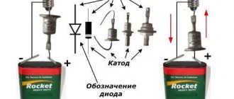
Note! There are two-terminal networks of direct polarity, when the anode is on the base, and reverse polarity, when the cathode is on the base.
Pin design with flexible (a) and rigid lead (b)
Housings of a flange design differ from a pin design in the absence of a pin and the external shape of the base in the form of a flange. Features of the pin and flange designs of diodes contribute to the process of one-sided cooling of their structure. These two-terminal networks are used for currents of 320-500 A.
The tablet housing is adapted for connecting heat sinks and current conductors to the base by means of a clamping device. This design allows for one-way and two-way heat removal from the structure of the device. Used at currents of 250 A and above.
Press-fit housing design with flexible (a) and rigid (b) leads
The press-fit diode body consists of a hollow cylinder with a corrugated surface and a bottom - the base on which the semiconductor structure is located. The second end of the cylinder is closed using a bushing with a flexible or rigid lead.
Double-terminal circuits in press-fit housings are produced in direct polarity when the anode is on the base, and in reverse polarity when the cathode is on the base. The press-fit housing provides for one-sided cooling of the semiconductor and is used for currents up to 25 A.
Modular designs of semiconductor two-terminal devices consist of a base with an insulating heat-conducting gasket, on which one or more semiconductor structures are located, and a protective housing with electrical leads. The base of the device, which provides heat removal, is produced electrically isolated from the terminals of the semiconductor structures included in the module. Modular designs are manufactured in different combinations of semiconductors for currents up to 160 A.
Other types
Selenium rectifiers, inferior to devices made of silicon and germanium in many respects, have unique self-healing capabilities in the event of a breakdown. There is no short circuit where selenium burns out.
Additional Information. The radiation resistance of selenium valves is much higher than that of other rectifiers.
Copper oxide rectifiers are characterized by low reverse voltage, low operating temperature, and low ratio of forward and reverse resistance.
Note! Currently, these valves are no longer used, as more advanced rectifier semiconductor devices have appeared on the market.
Usage
Semiconductor diode, a two-electrode electronic device based on a semiconductor (SC) crystal. The concept of "P. d." combines various devices with different principles of operation, having a variety of purposes. The classification system for semiconductor devices corresponds to the general classification system for semiconductor devices. The most common class of electrical transformer diodes includes: rectifier diodes, pulse diodes, zener diodes, and microwave diodes (including video detectors, mixing detectors, parametric detectors, amplifier and generator diodes, multipliers, and switching detectors). Among optoelectronic devices, photodiodes, light-emitting diodes, and PP quantum generators are distinguished.
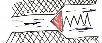
The most numerous are PDs, the action of which is based on the use of the properties of the electron-hole transition (p-n junction). If a voltage is applied to the p-n junction of the diode (Fig. 1) in the forward direction (the so-called forward bias), i.e., a positive potential is applied to its p-region, then the potential barrier corresponding to the junction decreases and begins intense injection of holes from the p-region into the n-region and electrons from the n-region into the p-region - a large forward current flows (Fig. 2). If a voltage is applied in the opposite direction (reverse bias), the potential barrier rises and only a very small minority carrier current flows through the pn junction (reverse current). In Fig. Figure 3 shows an equivalent circuit of such a P.D.
The operation of rectifier (power) diodes is based on the sharp asymmetry of the current-voltage characteristic (VC). For rectifier devices and other high-current electrical circuits, rectifier power supply units are produced that have a permissible rectified current Iv of up to 300 A and a maximum permissible reverse voltage U*rev from 20-30 V to 1-2 kV. Pds of similar application for low-current circuits have Iв < 0.1 a and are called universal.
At voltages exceeding U*o6p, the current increases sharply, and an irreversible (thermal) breakdown of the p-n junction occurs, leading to the failure of the p-n junction. In order to increase U*rev to several tens of kV, rectifier columns are used, in which several identical rectifier P.D. are connected in series and mounted in a common plastic housing. The inertia of rectifier diodes, due to the fact that the lifetime of the injected holes is > 10-5-10-4 sec, limits the frequency limit of their use (usually to the frequency range 50-2000 Hz). The use of special technological methods (mainly the doping of germanium and silicon with gold) made it possible to reduce the switching time to 10–7–10–10 sec and to create high-speed pulsed pulse generators, which are used, along with diode matrices, mainly in low-current signal circuits of computers.
It will be interesting➡ What is an LED
Diode marking
Diode 1n4007
The designation system for semiconductor diodes includes a code consisting of letters and numbers.
Device marking
The first component of the marking can be presented in the form of a number for devices of special purpose or in the form of a letter for devices of general use.
If the material designation uses:
- G or 1, then this is germanium and germanium compounds;
- K or 2, this is silicon and silicon compounds;
- A or 3 – gallium arsenide;
- And or 4 – indium phosphide.
To indicate the second digit in the marking, use:
- D – rectifier, pulse;
- C – in rectifying pillars and bridges;
- B – in the designation of varicaps;
- And - in tunnels;
- A – in the microwave;
- C – in zener diodes and stabilizers;
- G – in noise generators;
- L - in emitting LEDs.
The third element characterizes the main features of the device and depends on its subclass. For example, 2D204V is a silicon rectifier diode with a constant and average current value of 0.3-10 A, development number 04, group B.
Diode design
One possible diode design is shown below:
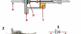
Let's consider one of the possible designs of the device. A semiconductor crystal 1 (for example, with electronic conductivity) is placed on a metal base 3. On the top of the crystal there is an impurity 2 (for example, indium), which ensures the presence of hole conductivity. The crystal is closed by housing 4 to avoid various mechanical damage to the pn junction.
An insulated output is made from the indium surfacing through glass insulator 5 - this is the anode of the device. The output of the cathode will be a metal housing 3, which also provides heat removal during operation of the device, thereby protecting it from thermal breakdown and overheating.
In turn, semiconductor elements are divided into:
- Low power – current up to 0.3 A;
- Average - from 0.3 to 10 A;
- Powerful - from 10 A;
Advantages of direct inclusion in the scheme
Including semiconductor devices directly into the circuit provides guaranteed advantages:
- High-quality signal processing;
- Full interchangeability of devices;
- Miniature and durable use;
- Ease of installation and replacement;
- Availability of purchase and low prices.
Additional Information. You can choose not only a domestic, but also a foreign analogue of a semiconductor device.
Advantages
Semiconductor diodes, when directly included in a circuit, provide the following advantages:
- Absolute interchangeability of various samples;
- High quality signal processing;
- Miniature and durable;
- Ease of installation and replacement;
- Availability and low cost.
All of the above advantages have turned these semiconductor parts into one of the most popular and sought-after elements used in the design of most modern radio equipment. The convenience of working with them is also manifested in the ease of selecting a suitable analogue (domestic or foreign).
Current-voltage characteristics (ideal and real)
The VA characteristic is given in the form of the relationship between the current of the external circuit of the pn junction of the device and the polarity of the voltage on its electrodes. This relationship can be obtained experimentally or calculated based on the current-voltage characteristic equation.
Ideal characteristic
The main task of a rectifier diode is to conduct electric current in one direction and prevent it from passing in the opposite direction. Therefore, when voltage is applied directly (plus is applied to the anode, and minus is applied to the cathode), the ideal device should be an excellent conductor, with a resistance equal to zero. With the opposite connection, on the contrary, it should have enormous resistance, becoming a complete insulator.
CVC of an ideal device
Additional Information. In practice, the ideal model is used in digital electronics because in this field only the logical function of the device matters.
Real current-voltage characteristic
A real diode, due to the structure of the semiconductor, has many disadvantages in comparison with an ideal two-terminal device.
CVC of a real device
The parameters of industrial plastic elements differ significantly from those that, for convenience, are accepted as ideal. In reality, the nonlinear I-V characteristic shows large deviations in both current values and conversion slope. Therefore, the device can only withstand the loads represented by these limit values:
- Maximum direct rectified current;
- Reverse leakage current;
- Maximum forward and reverse voltage;
- Potential drop at the pn junction;
- The maximum operating frequency of the processed signal.
The current-voltage characteristic for diode elements is an important parameter by which you can determine how the device will operate in an electrical circuit.
Important! Before using a two-terminal device for its intended purpose, you need to study the current-voltage characteristics of this device.
Common faults
Sometimes semiconductor devices stop functioning, which is explained by natural depreciation or the end of the established operational life. There are other types of faults, which include:
- Transition breakdown. With this phenomenon, the semiconductor becomes an ordinary conductor that does not have established properties and does not hold electric current in the established direction. You can solve the problem using a standard multimeter that beeps and determines the resistance level.
- Transition break. It is a reverse process, as a result of which the device turns into an insulator. Electric current in this case is passed in only one direction. To determine the location of the break, you need to use a tester with working probes. If these elements are not of sufficient quality, then it will not be possible to carry out an accurate and correct diagnosis.
- Violation of tightness. Any leakage is a serious threat to the normal operation of semiconductor devices.
Video
Coffee capsule Nescafe Dolce Gusto Cappuccino, 3 packs of 16 capsules
1305 ₽ More details
Coffee capsules Nescafe Dolce Gusto Cappuccino, 8 servings (16 capsules)
435 ₽ More details
Glass break sensors