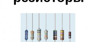
Content
- 1. General part
- 2. Determination of parameters of protective chains
- 2.1 Zener diode
- 2.2 Diode resistor
- 2.3 Protection diode
- 2.4 Selection of protective RC chain
- 2.5 Selection of protective circuit diodes
- 3. The influence of protective circuits on increasing the current load on switched contacts
- 4. Safety chains recommended for use
- 5. Method for reducing switching overvoltages when using a transistor as a switching element
- 6. Examples of choosing diode protection against switching overvoltages
- 7. Selecting a security chain
- 8. Selection of security chain parameters
- 8.1 Diode selection
- 8.2 Selection of resistors
- 9. References
a common part
Switching of relay windings in DC circuits of relay protection and automation is usually accompanied by significant overvoltages, which can pose a danger to the semiconductor devices used in these circuits. To protect transistors operating in switching mode, protective chains began to be used (Fig. 1), which are connected in parallel to the winding of a switched relay (Fig. 2 - here the winding of a switched relay is represented by an equivalent circuit - inductance L, active component of resistance R and the resulting interturn capacitance C ) and reduce overvoltages that occur between winding terminals 1 and 2.
Fig. 1 - Protective circuits used to reduce switching overvoltages
Fig. 2 - Protecting the VT transistor using a protective chain
However, at present, sufficient attention is not given to determining the parameters of protective chains and assessing their impact on the operation of relay protection devices. In addition, when developing and designing relay protection devices using semiconductor diodes exposed to switching overvoltages, in many cases diode protection is not provided.
This leads to quite frequent failure of the diodes and failure or incorrect operation of the device. An example of circuits where the diode can be affected by overvoltages is the circuit shown in Fig. 3. Here, the separating diode VD is exposed to switching overvoltage and can be damaged when the contacts KI are open and the contacts K2 are closed. To protect this diode, a protective circuit must be connected to terminals 1 and 2 of the winding of relay K3. To protect diodes, the same protective equipment can be used that is used to protect transistors (Fig. 1).
Fig. 3 - Circuits in which the diode VD may be exposed to switching overvoltages
Purpose of TVS diodes
| TVS diode marking | Application of TVS diodes |
| P4SMAJ5.0A | unipolar, for protecting 5V DC power circuits |
| P4SMAJ5.0CA | bipolar, for AC or signal circuits |
| P4SMAJ14A 1.5SMC16A | unipolar, for 12V stabilized DC power supply circuits |
| 1.5SMC18A | unipolar, to protect 12V power circuits when using the vehicle’s on-board network |
| 1.5SMCJ28A | unipolar, to protect 24V power circuits when using the vehicle’s on-board network |
Protection diodes operate on a reversible avalanche breakdown of a semiconductor junction, so they are rightly called avalanche diodes. Avalanche diodes are used for surge protection in power supply circuits of electronic equipment. Together with gas arresters and varistors they provide lightning protection of electrical equipment. To protect against surge voltage and static electricity, a single ESD suppressor or a multi-channel protective diode assembly is used in the data transmission interfaces. Protection of power circuits from excess current consumption is carried out by fuses. There are disposable fuses and reusable self-resetting fuses.
Technical characteristics of protection diodes in SMA
Technical characteristics of protection diodes in SMC
The manufacturer of TVS suppressor diodes is PANJIT.
A suppressor, also known as a PON (semiconductor voltage limiter), also known as a TVS diode (Transient Voltage Suppressor), also known as a protective diode, also known as a diode fuse, allows you to protect equipment from overvoltage.
Each suppressor has a voltage rating (typically 6.8 to 440 volts). As long as the voltage at its terminals does not exceed the rated voltage, it does not have any effect on the operation of the circuit. As soon as the amplitude of the electrical pulse exceeds the rated voltage, the suppressor will switch to avalanche breakdown mode and limit the voltage pulse to the rated value.
Suppressors are available both asymmetrical (unidirectional) and symmetrical (bidirectional). Unidirectional suppressors are designed to operate in circuits with constant voltage of the same polarity. Bidirectional can operate in circuits with bipolar or alternating voltage.
In the diagrams, the suppressor is designated as follows (bidirectional on the left, unidirectional on the right):
Suppressors are marked as follows:
So, for example, a suppressor marked P6KE6.8A is unidirectional with a nominal voltage of 6.8 volts and a peak power of 600 watts (such suppressors are used in good 5-volt chargers), and a suppressor marked 1.5KE440CA is bidirectional with a rated voltage of 440 volts and a peak power of 1500 watt (such suppressors are used to protect devices powered by a mains voltage of 230 volts).
The main advantages of the suppressor are a very short reaction time to overvoltage and the ability to dissipate very high power without destruction. The suppressor is able to “take the hit” for a short time. To suppress high-voltage impulse noise in the network or to trigger protection in the power supply, this is enough, but if there is a possibility that the overvoltage may persist for a long time, the suppressor is used together with a fuse that will simply blow out during a prolonged overvoltage and protect the circuit from failure.
Determining the parameters of protective chains
The values of the parameters of the protective circuits are determined based on the condition of reducing the impact of overvoltages on the protected semiconductor device to an acceptable level. This is achieved by creating an additional circuit for the current passing in the relay winding.
The switching overvoltage Up, affecting the semiconductor device during the transient process, is defined as [L1]:
Up= Uс+E (1)
Where:
- E – voltage of the operational current power supply;
- Uс – switching overvoltage on the relay winding.
Overvoltage Uп must comply with the condition [L2]:
Up < 0.7*Uadd (2)
where: Uadd is the maximum permissible voltage value of the semiconductor device.
Based on equality (1), the maximum permissible voltage on the winding of a switched relay in the case of using protective circuits:
Um=0.7Uadd.-E (3)
Condition (3) is the starting point for determining the parameters of the protective chains:
2.1 Zener diode
When using a Zener diode protective circuit, the stabilization voltage is equal to Um, determined from equality (3).
2.2 Diode resistor
The resistor resistance values when switching a number of relays common in relay protection and automation technology are determined using the curves shown in Fig. 4 and correspond to the point of intersection of the curve Uм=f(Rp) with a straight line (0.7*Uadd.-E) parallel to the axis Rр. The curves were obtained by measuring overvoltages using a beam oscilloscope using a high-resistance ohmic voltage divider. The power of the resistor does not play a significant role and 1-2 Watts can be taken.
Fig.4 a) - Dependence Um=f(Rp) for relays: RP-23/220 (curve 1), RP-252/220 (curve 2), relays of the EV100 series (without spark-extinguishing circuit, (curve 3)
Fig.4 b) - Dependence Um=f(Rp) for relay RU21/220
Fig. 4 c) - Dependence Uм=f(Rp) for relays: RPU-2/220 (curve 1), RP222-U4/220 (curve 2), RP255/220 (curve 3), RP251/220 (curve 4 )
2.3 Protection diode
When using a protective diode Uc = 0 and the voltage on the protected semiconductor device according to (1) Uп = E.
2.4 Selection of protective RC chain
The value of resistance R (the resistance of the RC circuit resistor) is determined from the condition of limiting the current load on the switching contacts from the charging current of the capacitor C3 (the capacitance of the RC circuit capacitor) by the permissible load, i.e.
Ioz=E/Rz < Iadd. (4)
The resistance of the RC chain resistor, based on the permissible switching capacity of the contacts most common in protection and automatic relay devices, can be taken with a sufficient margin of 2 kOhm, and the power - 1-2 Watts.
The value of capacitance Cz is determined graphically and corresponds to the point of intersection of the dependence curve Um=f(Cz) with a straight line (0.7*Uadd.-E) parallel to the Cz axis (see Fig. 5).
Rated voltage Unom. capacitance Сз must comply with the condition E < 0.7*Unom.
Fig.5 a) - Dependence Uм=f(Сз) for relays: RP-252/220 (curve 1), RU21/220 (curve 2)
Fig.5 b) - Dependence Uм=f(Сз) for relays: RP-251/220 (curve 1), RP222-U4/220 (curve 2), RPU-2/220 (curve 3)
Fig.5 c) - Dependence Uм=f(Сз) for relays: RP-23/220 (curve 1), relay of the EV100 series (without spark-extinguishing circuit, (curve 2), RP-255/220 (curve 3)
2.5 Selection of protective circuit diodes
The selection of diodes for protective circuits is made according to the maximum permissible voltage of the diodes, based on the condition:
E < 0.7*Uadd. (5)
The influence of protective circuits on increasing the current load on switched contacts
The protective circuits under consideration practically do not increase the current load on the switching contacts: if there is a semiconductor diode in the protective circuit, the current load increases by the amount of the reverse current of the diode, which, having a value of up to several tens of microamperes, is very small compared to the current in the relay winding. The additional load on the switching contacts in the case of using a protective RC circuit is determined by the active leakage current of the capacitor, which is also very small and can not be taken into account. It should be noted that protective chains, by reducing the magnitude of switching overvoltages, facilitate the operating conditions of switching contacts.
What it is
The literature gives the following definition:
A Zener diode or Zener diode is a device designed to stabilize voltage in electrical circuits. Operates under reverse bias in breakdown mode. Before breakdown occurs, it has a high transition resistance. The currents flowing in this case are insignificant. Widely used in electronics and electrical engineering.
In simple terms, a zener diode is designed to stabilize voltage in electronic circuits. It is connected to the circuit in the opposite direction. When a voltage exceeds the stabilization voltage, a reversible electrical breakdown of the pn junction occurs. As soon as it drops to nominal, the breakdown stops and the zener diode closes.
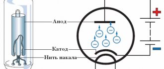
The figure below is a graphical diagram for dummies to help you understand the working principle of a Zener diode.
The main advantages are low cost and small dimensions. The industry produces devices with stabilization voltages of 1.8 - 400 V in metal, ceramic or glass cases. This depends on the power for which the zener diode is designed and other characteristics.
To stabilize high-voltage voltages from 0.4 to several tens of kV, glow discharge zener diodes are used. They have a glass body and, before the advent of semiconductor devices, were used in parametric stabilizers.
Devices that change their resistance depending on the applied voltage have similar properties - these are varistors. The difference between a zener diode and a varistor is that the latter has bidirectional symmetrical characteristics. This means that, unlike diodes, it has no polarity. Briefly, a varistor is designed to provide overvoltage protection to electronic circuits.
Suppressors are used to protect equipment from power surges. The differences between a zener diode and a suppressor are that the former gradually changes its internal resistance depending on the applied voltage. The second one opens immediately when a certain voltage threshold is reached. Those. its internal resistance tends to zero. The main purpose of suppressors is to protect equipment from power surges.
The figure below shows the conventional graphic designation (UGO according to GOST) of a semiconductor and its current-voltage characteristic.
The numbers in the figure indicate area 1-2. It is working and is designed to stabilize voltage in circuits. If the device is turned on in the forward direction, it will work like a regular diode.
We recommend watching the following video to learn more about the principle of operation of a zener diode, the designation of elements and their scope of application.
Examples of choosing diode protection against switching overvoltages
Figures P-1a - P-5a show the practically used circuit diagrams of direct current relay protection circuits with separating diodes. In some of these circuits, the decoupling diodes may be subject to switching overvoltages.
1. Fig. A-1a When contacts K1 are closed and contacts K2 are open, almost all the current in the winding of relay K4 is turned off. In this case, a switching overvoltage occurs between the terminals of the winding of relay K4 (in winding K4 the reverse saturation current of the diode VD, amounting to several microamps, continues to flow), and the potential of the positive terminal of the winding becomes much lower than the potential of the negative pole of the power source. The diode VD is exposed to a reverse voltage that exceeds the maximum permissible voltage of the D229B diode.
Fig.P-1a - K3, K4 - relay windings, respectively RP255/220, RP251/220; VD, VD1 - diodes D229B; VD1,R - safety chain
2. Fig. P-2a. Diodes VD1, VD2 are exposed to switching overvoltage when contacts K1 are closed and contacts K2 are open, since almost all the current in the relay winding K6 is turned off, and the potential of its positive terminal is much lower than the potential of the negative pole.
Fig.P-2 - K3, K4, K5 - relay windings RP252-U4/220; K6 - relay winding RPU-2/220; VD1-VD6 - diodes D229B; VD5,R4 - spark arresting circuit; VD6,R5 - protective chain
3. Fig. P-3a. When the current in the winding of relay K7 is switched off by contacts K2, when contacts K1 are in the closed position, the transient process occurs similarly to that discussed above. Switching overvoltage affects diodes VD1, VD2.
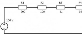
Fig.P-3 - K3 - indicating relay winding; K4, K5, K6 relay windings RP252-U4/220, K7 - relay winding RPU-2/220; VD1-VD6 - diodes D229B; R1, R2 - resistors, respectively, 3000 and 2000 Ohms; VD5,R6 - spark arresting circuit; VD6,R7 - protective chain; SX - overlay
4. Fig. P-4. In this circuit, the separating diodes are not exposed to switching overvoltages.
Fig.P-4 - K3, K4 - windings of indicating relays; K5 - series winding of the intermediate relay; K6, K7 relay windings RP222-U4/220; VD1, VD2 - diodes D229B; R - 1000 Ohm resistor;
5. Fig. P-5a. Diode-resistor chains connected in parallel to the relay windings (see also Fig. P-2a, P-3a) and designed to reduce sparking at the contacts, to some extent limit the switching overvoltage on the separating diodes. The use in these chains of two, instead of one, series-connected diodes with resistors connected in parallel to them (serving to uniformly distribute the reverse voltage across the diodes) was undertaken in order to prevent breakdown of the diodes of these chains from the effects of overvoltages.
However, the possibility of the influence of switching overvoltage on the diodes-resistor chains in the circuit of Fig. P-5a (as well as in circuits P-2a, P-3a) is excluded (It is assumed that overvoltages cannot also enter the circuit of Fig. P-5a from the source side nutrition). Therefore, it is advisable to replace all these relatively complex chains with diode-resistor chains (Fig. P-2b, P-3b, P-5b). Moreover, if the probability of a break in the circuit of separating diodes is insignificant, it is possible to use instead of three one common diode-resistor circuit, connecting it in parallel with the winding of relay K8 (Fig. P-5c).
The common diode-resistor protective circuit, along with a reduction in the level of switching overvoltages affecting the separating diodes VD1-VD4, helps reduce sparking at the contacts.
Fig.P-5 - K4, K5 - relay windings RP223/220; K6, K7, K8 - relay windings RP23/220; VD1-VD14 - diodes D229B; R1 - 1000 Ohm resistor;
Operating principles
The protective diode has a specific VA characteristic characterized by nonlinearity. Provided that the size of the pulse amplitude is greater than permissible, this will entail a so-called “avalanche breakdown”. In other words, the amplitude size will be normalized, and all excess will be removed from the network through a protective diode.
Fig. 1 Protective diode - principle of operation of a semiconductor
The operating principle of a TVS diode assumes that until a danger occurs, the diode fuse in no way affects the device itself or its functional properties. Thus, it should be noted that another name for the protective diode is emerging - an avalanche diode.
There are two types of limiting zener diodes:
Symmetrical.
Protective diode, bidirectional, suitable for operation in alternating current networks.
Asymmetrical.
Applicable only for networks with direct current, since they have a unidirectional operating mode. The method of connecting an asymmetrical protective diode does not correspond to the standard. Its anode is connected to the negative bus, and its cathode is connected to the positive bus. The position turns out to be conditionally inverted.
The coding of protective diodes classified as symmetrical includes the letters “C” or “CA”. Single-ended diode fuses have a color-coded stripe on the cathode terminal side.
The housing of each protective diode is also equipped with a marking code that displays all significant parameters in a compressed form.
If the input voltage level of the diode increases, the zener diode will reduce its internal resistance over a very short period of time. The current strength at this moment, on the contrary, will increase, and the fuse will blow. Since the protective diode acts almost instantly, the integrity of the main circuit is not compromised. In fact, a quick response to excess voltage is the most important advantage of a TVS diode.
Selecting security chain parameters
8.1 Diode selection
Protective circuit diodes are selected based on the following conditions:
E < 0.7*Uadd. (5)
Considering that E = 220 V, we choose a diode of type D229B, which has Uadd = 400 V.
8.2 Selection of resistors
The resistor resistance values are determined using the curves in Fig. 4 and correspond to the intersection point of the curve Uм=f(Rp) with the straight line 0.7*Uadd.-E=0.7*400-220=60V, parallel to the Rр axis.
In the circuits presented in Fig. P-1b, P-2b, P-3b, the resistance of the protective circuit resistor is determined from the curves for relays RP-251, RPU-2 and are respectively equal to R = 2.4 kOhm, R5 = 4.2 kOhm , R7=4.2 kOhm.
The design case for the circuit in Fig. P-5c is the case of disconnection by contacts K3 of three parallel-connected relay windings K6, K7, K8 with the contacts K1 in the closed position. Moreover, if there is no protective circuit in the circuit in Fig. P-5c, then diodes VD1, VD2 are exposed to switching overvoltage. The resistance of the protective circuit resistor is defined as equivalent to three equal resistances connected in parallel, one of which (Rр) is determined from the curve in Fig. 4 for the RP-23 relay:
R2=Rр/3=2.2/3=0.773 kOhm
In the diagram shown in Fig. P-5c, it is worthy of attention to consider the possibility of relay K8 operating when contacts K2 are opened. The answer to this question in the case under consideration can be obtained by comparing the maximum value of the current passing through the winding of relay K8 in the transient mode with the minimum operating current of this relay. The current I passing in the winding of relay K8 when the contacts K2 is opened is the sum of current I1, which represents part of the sum of the currents in the windings of relays K4, K5 and current I2 - part of the sum of the currents in the windings of relays K6, K7. The maximum values of currents I1, I2, I are determined as follows:
Here: Ik4, Ik5, Ik6, Ik7 are the currents passing respectively in the relay windings K4, K5, K6, K7.
Where:
- 220 – power supply voltage (V);
- 9300, 9250 – direct current resistance, respectively, of the RP-23 relay winding and the RP-223 relay winding connected in series with the additional resistor (Ohm).
Minimum operating current of relay K8 (RP-23):
Thus, the amount of current passing in the winding of relay K8 when contacts K2 opens is insufficient to trigger the relay (If Im > Iav.k8, then relay K8 will operate when the condition tb > tav is met, where:
- tav – time during which Im > Iav.k8;
- tb – response time of relay K8.
Two-hit hypothesis
Unlike oncogenes, tumor suppressor genes generally follow the two-hit hypothesis, which states that both alleles encoding a particular protein must be affected before the effect is seen. If only one allele of a gene is damaged, the other may still produce enough of the correct protein to maintain the corresponding function. In other words, mutant alleles for tumor suppressors are usually recessive, whereas mutant alleles for oncogenes are usually dominant.
Tumor suppression models
The two-hit hypothesis was first proposed by A.G. Knudson for cases of retinoblastoma. He noted that 40% of cases in the United States were caused by a germline mutation. However, affected parents may have children without the disease; but healthy children became parents of children with retinoblastoma. This indicates that it is possible to inherit a mutated germline but not manifest the disease. Knudson noted that the age of onset of retinoblastoma follows , implying that two independent genetic events are required. He recognized that this corresponded to a recessive mutation involving a single gene, but required a biallelic mutation. Hereditary cases include an inherited mutation and a single mutation of the normal allele. Non-hereditary retinoblastoma involves two mutations, one for each allele. Knudson also noted that hereditary cases often develop bilateral tumors, and they will develop earlier, compared to non-hereditary cases where people were affected by only one tumor.
There are exceptions to the two-hit rule for tumor suppressors, such as certain mutations in the p53 gene product. p53 mutations can function as dominant negatives, meaning that the mutated p53 protein can interfere with the natural protein produced by the non-mutant allele. Other tumor suppressor genes that do not follow the two-hit rule are those that exhibit haploinsufficiency, including PTCH in medulloblastoma and NF1 in neurofibroma. Another example is p27, a cell cycle inhibitor that, when mutated on one allele, causes increased susceptibility to carcinogens.