Main characteristics of diodes
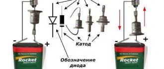
First, let's remember what a regular diode is and how it works. This is a semiconductor device that consists of two zones. Under certain conditions, electrons move through this transition.
Diode design and designation
The main property of the element is that it allows current to pass in one direction and not in the other. Schottky diodes have the same characteristics as conventional ones. Let’s focus on some in more detail. These are voltage drop, reverse current, reverse voltage, frequency.
Schottky diode is different from conventional silicon diodes
Schottky diodes are made from silicon (Si), gallium arsenide (GaAs), and rarely germanium (Ge). The metal in connection with the semiconductor determines many of the parameters of the diode. This metal may be gold (Au), rallyadium (Pd), platinum (Pt), tungsten (W) which is deposited on semiconductors.
And just like a regular diode, the semiconductor-metal connection has one-way conductivity with a number of positive as well as negative qualities.
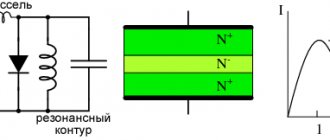
Current-voltage characteristic of a Schottky diode
The current-voltage characteristic of a Schottky diode differs from a conventional semiconductor diode by being more nonlinear.
What are the benefits of using a metal-semiconductor connection? Two positive points:
- A very small voltage drop across the direct junction is 0.2-0.4 V. For a silicon diode, the “average” value of this parameter is 0.7 V. However, only devices with a low breakdown voltage - up to 100 V have a low voltage drop. For more powerful ones, the drop is only slightly lower than for silicon ones.
- High performance. That is, he quickly changes his state. The transition from an open state to a closed state and back occurs in a very short period of time and is determined only by the barrier capacitance. They are used in switching systems where response speed is important.
What is a Schottky diode and how is it indicated in the diagram
They also have disadvantages. As the temperature rises, their reverse current increases significantly.
The second drawback is that if the maximum permissible reverse voltage is exceeded, an irreversible breakdown occurs. That is, the device fails. There is one more disadvantage - the low forward voltage drop is only found in Schottky diodes with a low breakdown voltage (up to hundreds of volts). Higher voltage variants have losses comparable to silicon ones.
Designation, application and parameters of Schottky diodes
To the large family of semiconductor diodes named after the names of the scientists who discovered the unusual effect, we can add one more.
This is a Schottky diode. German physicist Walter Schottka discovered and studied the so-called barrier effect that occurs with a certain technology for creating a metal-semiconductor transition.
The main feature of a Schottky diode is that, unlike conventional diodes based on a pn junction, it uses a metal-semiconductor junction, which is also called a Schottky barrier. This barrier, just like the semiconductor pn junction, has the property of one-way electrical conductivity and a number of distinctive properties.
The materials used to make Schottky barrier diodes are predominantly silicon (Si) and gallium arsenide (GaAs), as well as metals such as gold, silver, platinum, palladium and tungsten.
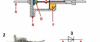
In circuit diagrams, a Schottky diode is depicted like this.
As you can see, its image is somewhat different from the designation of a conventional semiconductor diode.
In addition to this designation, in the diagrams you can also find an image of a dual Schottky diode (assembly).
A dual diode is two diodes mounted in one common housing. The terminals of their cathodes or anodes are combined. Therefore, such an assembly, as a rule, has three outputs. Switching power supplies usually use common cathode assemblies.
Since two diodes are placed in the same housing and made in a single technological process, their parameters are very close. Since they are placed in a single housing, their temperature conditions are the same. This increases the reliability and service life of the element.
Schottky diodes have two positive qualities: a very low forward voltage drop (0.2-0.4 volts) across the junction and very high performance.
Unfortunately, such a small voltage drop occurs when the applied voltage is no more than 50-60 volts. As it increases further, the Schottky diode behaves like a regular silicon rectifier diode. The maximum reverse voltage for Schottky usually does not exceed 250 volts, although on sale you can find samples rated at 1.2 kilovolts (VS-10ETS12-M3).
Thus, the dual Schottky diode (Schottky rectifier) 60CPQ150 is designed for a maximum reverse voltage of 150V, and each of the diodes in the assembly is capable of passing 30 amperes in direct connection!
You can also find samples whose half-cycle rectified current can reach a maximum of 400A! An example is the VS-400CNQ045 model.
Very often, in circuit diagrams, the complex graphical representation of the cathode is simply omitted and the Schottky diode is depicted as a regular diode. And the type of element used is indicated in the specification.
The disadvantages of diodes with a Schottky barrier include the fact that even if the reverse voltage is briefly exceeded, they instantly fail and, most importantly, irreversibly. While silicon power valves, after the excess voltage stops, are perfectly self-healing and continue to work. In addition, the reverse current of diodes very much depends on the junction temperature. At a large reverse current, thermal breakdown occurs.
In addition to high speed and, therefore, short recovery time, the positive qualities of Schottky diodes include a small junction (barrier) capacitance, which allows you to increase the operating frequency. This allows them to be used in pulse rectifiers at frequencies of hundreds of kilohertz. A lot of Schottky diodes find their application in integrated microelectronics. Schottky diodes made using nanotechnology are included in integrated circuits, where they bypass transistor junctions to improve performance.
Schottky diodes of the 1N581x series (1N5817, 1N5818, 1N5819) have taken root in amateur radio practice. All of them are designed for a maximum forward current ( IF(AV) ) of 1 ampere and a reverse voltage ( VRRM ) of 20 to 40 volts. The voltage drop ( VF ) across the junction is 0.45 to 0.55 volts. As already mentioned, the forward voltage drop of diodes with a Schottky barrier is very small.
Another fairly well-known element is 1N5822. It is designed for a forward current of 3 amperes and is housed in a DO-201AD housing.
Also on printed circuit boards you can find diodes of the SK12 - SK16 series for surface mounting. They are quite small in size. Despite this, SK12-SK16 can withstand forward current up to 1 ampere at a reverse voltage of 20 - 60 volts. The forward voltage drop is 0.55 volts (for SK12, SK13, SK14) and 0.7 volts (for SK15, SK16). Also in practice you can find diodes of the SK32 - SK310 series, for example, SK36 , which is designed for a forward current of 3 amperes.
Application of Schottky diodes in power supplies.
Schottky diodes are actively used in computer power supplies and switching voltage stabilizers. Among the low-voltage supply voltages, the highest current (tens of amperes) are +3.3 volts and +5.0 volts. It is in these secondary power supplies that Schottky barrier diodes are used. Most often, three-terminal assemblies with a common cathode are used. It is the use of assemblies that can be considered a sign of a high-quality and technologically advanced power supply.
Failure of Schottky diodes is one of the most common faults in switching power supplies. It can have two “dead” states: pure electrical breakdown and leakage. If one of these conditions is present, the computer's power supply is blocked as the protection is triggered. But this can happen in different ways.
Application in electronics
Properties such as speed and low voltage drop allow the use of Schottky diodes in high-frequency circuits. For example, in high-frequency power rectifiers (up to hundreds of kilohertz), where they work as high-frequency rectifiers. They are also used in sound amplifiers, since compared to conventional diodes they produce a lower level of interference.
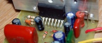
If you look at the power supply board, you will definitely see a Schottky diode
Another application is as an integral part of more complex semiconductor devices. For example, MOS transistors, diode assemblies and power diodes with a built-in Schottky diode have better characteristics.
The scope of application of the products is wide, but they are most often used in computer power supplies. And also in circuits for modulating light in radiation receivers and solar batteries.
Nomenclature of Schottky diodes [edit | edit code]
Schottky diodes are components of modern discrete semiconductor devices:
- MOSFETs with a built-in freewheeling Schottky diode (first released by International Rectifier under the FETKY brand in 1996) are the main component of synchronous rectifiers. Unlike a conventional MOS transistor, the reverse diode of which is characterized by a high forward voltage drop and mediocre time characteristics (since it is a conventional pn junction diode formed by the drain regions and the substrate combined with the source), the use of a reverse Schottky diode allows you to build power synchronous rectifiers with conversion frequencies of hundreds of kHz and higher. There are devices in this class with built-in gate drivers and synchronous rectification control devices.
- The so-called ORing [3] diodes and ORing assemblies are power diodes and diode assemblies used to combine parallel power supplies for a common load in high-reliability devices (logical OR power supply). They are distinguished by a particularly low, standardized forward voltage drop. For example, a specialized miniature diode MBR140 (30 V, 1 A) at a current of 100 mA has a forward voltage drop of no more than 360 mV at +25 °C and 300 mV at +85 °C. ORing diodes are characterized by a relatively large pn junction area and low specific current densities.
Symbol and characteristics
In the diagram, the Schottky diode has a special designation. The difference from the usual one is that the crossbar of the triangle has curved edges. Not one, like a zener diode, but both. And these edges are bent in different directions. The figure shows the designation according to GOST.
Schottky diode in the diagram: symbol
We have already talked about the characteristics. These are three main parameters:
- Voltage drop during forward transition. For Schottky diodes it is lower than for conventional silicon diodes. With a reverse breakdown power of up to 100 V, it will be on the order of 0.2-0.4 V (for silicon on average 0.6-0.7 V).
- Breakdown voltage. The usual value is up to 200 V, but there are also products with voltages of more than 1000 volts.
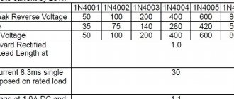
Parameters of the popular series of Schottky diodes 1N58**
- Reverse current. Under normal conditions (up to 20 °C) it is not too high - about 0.05 mA, but as the temperature rises it increases sharply.
The given parameters are average. There is a fairly serious range and for each case you can select the necessary characteristics for each of the points. Sometimes such a parameter as switching speed (performance) is also important.
Schottky diodes: description, principle of operation, circuit, main parameters, application, characteristics
In the late 30s of the 20th century, German physicist Walter Schottky discovered that an external electric field forces free electrons to leave the conduction band and literally leave the solid body. This quantum dependence was subsequently named after its discoverer and is now known as the Schottky effect.
Despite the fact that the discovery of the German scientist belongs to the field of theoretical physics, it finds application in practical radio engineering and underlies the functionality of such radio components as Schottky diodes. Their difference from conventional electric valves is the absence of a classic semiconductor pn junction. Its role is played by the contact between the semiconductor and the metal.
Metal and semiconductor: contact features.
In the contact region of semiconductor and metal materials, the Schottky effect leads to the formation of a layer in the semiconductor that is highly depleted of electrons. It has the valve properties inherent in a semiconductor pn junction. This zone is a barrier to charge carriers, which is why these radio components are often called Schottky barrier diodes.
The elements differ from conventional semiconductor valves in the following qualities:
- reduced voltage drop at forward bias;
- insignificant own capacity;
- low reverse current;
- low permissible reverse voltage.
With forward bias, the potential difference across the Schottky diode does not exceed 0.5 V, while on a conventional rectifier valve the voltage drop is about 2-3 V. This is explained by the low resistance of the transition section between the semiconductor and the metal.
The good frequency characteristics of Schottky diodes are due to the absence of minority charge carriers in the transition zone. Because of this, the processes of diffusion and recombination of holes and electrons that are usual for a purely semiconductor pn junction do not occur in the contact region. Consequently, the intrinsic capacitance of this layer tends to zero. This property makes Schottky barrier diodes preferable for use in high- and ultra-high-frequency circuits, as well as equipment with pulsed operating modes - all kinds of digital devices, electronics control systems and switching power supplies.
Low voltage diodes.
The peculiarity of Schottky diodes is that they are low voltage. If the applied potential difference exceeds a certain permissible level, then, in accordance with quantum laws, a breakdown occurs, which in a conventional semiconductor radio component can be tunneling, avalanche or thermal. After the first two, the diode is restored and continues to work properly. Thermal breakdown means fatal failure.
In diodes with a Schottky barrier, breakdown is always only thermal. This is a feature of the metal-semiconductor junction. If the reverse bias is large, the element fails and needs to be replaced. This, by the way, explains the strong sensitivity of Schottky diodes to static electricity - when installing them and servicing radio equipment with these elements, it is necessary to ground protective clothing and tools.
However, the sensitivity of these radio components is not always their disadvantage. For example, due to this characteristic, Schottky barrier diodes are used in particularly sensitive local oscillators, which gain the ability to process radio signals of very low power.
Main parameters.
- Maximum constant reverse voltage;
- Maximum pulse reverse voltage;
- Maximum (average) forward current;
- Maximum pulse forward current;
- Constant forward voltage across the diode at a given forward current through it;
- Diode reverse current at maximum reverse voltage;
- Maximum operating frequency of the diode;
- Reverse recovery time;
- Total diode capacity.
Production of Schottky diodes.
Standard materials are used as semiconductor components - silicon, germanium and gallium arsenide. In the process of manufacturing radio components, metals such as gold, silver, palladium, and tungsten are sprayed onto them. It is these elements of the periodic table that provide a sufficiently high potential barrier that determines the functionality of Schottky diodes.
Germanium radio components show high resistance to temperature changes, so this material is more often used than silicon and gallium arsenide in the production of diodes for high-power power supply circuits. But silicon and gallium elements demonstrate better frequency parameters.
Types of Schottky diodes
Currently, this type of diode is usually used in electronic devices. There are the following types:
- Single.
- Twin with a common anode;
- with a common cathode;
Two housing options for dual Schottky diodes
- series connected.
Dual Schottky diodes (or diode assemblies) are made in one housing, similar to power switches, and have three terminals. The diodes in the assembly have the same or very similar parameters, since they are performed in the same technological cycle.
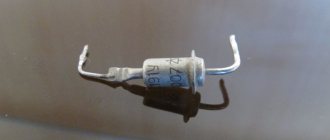
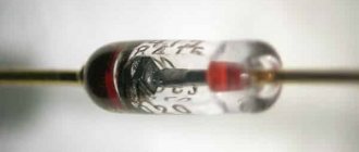
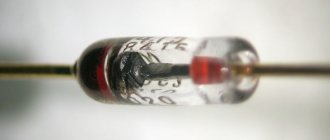
Often Schottky diodes look exactly like this, but there are also options in the form of regular diodes and SMDs. As you can see, on the plastic ones there is a designation for a bunch of two diodes - with a common anode
The part has a conventional body in the form of small cylinders with two wire leads. The cathode is marked with a stripe.
Table of names and characteristics
Schottky diodes are produced in certain series. There are not many manufacturers in the world, several dozen series. The table contains the most common elements of domestic and imported (non-Chinese) production.
| Domestic Schottky diodes | Imported Schottky diodes | U max, V | Imax, A | Type |
| 1N5817 | 20-25 | 1 | Single | |
| 1N5820 | 20-25 | 3 | Single | |
| KD269 A, AS | 20-25 | 5 | Single/double | |
| KD238AS | 20-25 | 7,5 | Twin | |
| KD270 A, AS | 20-25 | 7,5 | Single/double | |
| KD271 A, AS | 20-25 | 10 | Single/double | |
| KD272 A, AS | SR1620 | 20-25 | 15 | Single/double |
| KD273 A, AS | 20-25 | 20 | Single/double | |
| 1N5818 | 30-35 | 1 | Single | |
| 1N5821 | 30-35 | 3 | Single | |
| KD638 A, AS | 30-35 | 5 | Twin | |
| KD238 A, AS | 30-35 | 7,5 | Twin | |
| 10TQ0.5 | 30-35 | 10 | Single | |
| 12TQ035 | 30-35 | 15 | Single | |
| 20TQ035 | 30-35 | 20 | Single | |
| SR5030 | 30-35 | 50 | Twin | |
| 1N5819 | 40-45 | 1 | Single | |
| 1N5822 | 40-45 | 3 | Single | |
| KD638 AS | SR540 | 40-45 | 5 | Single |
| KD238 AS | 6TQ045 | 40-45 | 7.5 | Twin |
| 10TQ045 | 40-45 | 10 | Single | |
| 12TQ045 | 40-45 | 15 | Single | |
| 20TQ045 | 40-45 | 20 | Single | |
| SR350 | 50 | 3 | Single | |
| KD269 B, BS | 50 | 5 | Single/double | |
| KD270 B, BS | SR850 | 50 | 7.5 | Single/double |
| KD271 B, BS | 50 | 10 | Single/double | |
| KD272 B, BS | 50 | 15 | Single/double | |
| KD273 B, BS | 18TQ050 | 50 | 20 | Single/double |
| SR160 | 60 | 1 | Single | |
| SR360 | 60 | 3 | Single | |
| KD638 BS | SR560 | 60 | 5 | Twin |
| KD636 AS | SR1660 | 60 | 15 | Twin |
| KD637 AS | 60 | 25 | Twin | |
| KD269 V, VS | 50SQ080 | 75 | 5 | Single/double |
| KD270 V, VS | 8TQ060 | 75 | 7,5 | Single/double |
| KD271 V, VS | 75 | 10 | Single/double | |
| KD272 V, VS | 75 | 15 | Single/double | |
| KD273 V, VS | 75 | 20 | Single/double | |
| 30CPQ80 | 75 | 30 | Twin | |
| 11DQ09 | 90-100 | 1.1 | Single | |
| 31DQ10 | 90-100 | 3.3 | Single | |
| KD638 VS | 90-100 | 5 | Twin | |
| KD269 G, GS | 50SQ100 | 90-100 | 5 | Single/double |
| KD270 G, GS | 8TQ100 | 90-100 | 7.5 | Single/double |
| KD271 G, GS | 90-100 | 10 | Single/double | |
| KD272 G, GS | 90-100 | 15 | Single/double | |
| KD273 G, GS | 90-100 | 20 | Single/double | |
| 30CPQ100 | 90-100 | 30 | Twin | |
| KD638 GS | 150 | 5 | Twin | |
| KD269 D, DS | 150 | 5 | Single/double | |
| KD638 DS | 150 | 5 | Twin | |
| KD270 D, DS | 150 | 7,5 | Single/double | |
| KD271 D, DS | 10CTQ150 | 150 | 10 | Single/double |
| KD636 BS | 150 | 15 | Twin | |
| KD272 D, DS | 150 | 15 | Single/double | |
| KD273 D, DS | 150 | 20 | Single/double | |
| KD637 BS | 150 | 25 | Single/double | |
| 30CPQ150, SF303 | 150 | 30 | Twin | |
| UF4003, SF14 | 200 | 1 | Single | |
| SF24 | 200 | 2 | Single | |
| SF34, HER303 | 200 | 3 | Single | |
| KD369 E, EU | 200 | 5 | Single/double | |
| KD638 EU | 200 | 5 | Twin | |
| KD270 E, EU | 200 | 7,5 | Single/double | |
| KD271 E, EU | 200 | 10 | Single/double | |
| KD272 E, EU | 200 | 15 | Single/double | |
| KD638 VS | 200 | 15 | Twin | |
| KD273 E, EU | 200 | 20 | Single/double | |
| KD637 VS | 200 | 25 | Twin | |
| SF304, 30EPF02 | 200 | 30 | Single | |
| UF4004. SF16 | 400 | 1 | Single | |
| SF26 | 400 | 2 | Single | |
| SF26, HER305 | 400 | 3 | Single | |
| KD640 A, AS | 400 | 8 | Single/double | |
| KD271 K, KS, K1 | 10ETF04 | 400 | 10 | Single/double |
| KD272 K, KS, K1 | 16CTU04 | 400 | 15 | Single/double |
| KD641 A, AS | 400 | 15 | Single/double | |
| KD636GS | 400 | 15 | Twin | |
| KD273K, KS, K1 | 400 | 20 | Single/double | |
| KD637GS | 30CPF04 | 400 | 25 (30) | Twin |
| KD640 B, BS | 500 | 8 | Single/double | |
| KD640 E, EU | 500 | 8 | Single/double | |
| KD271 L, LS, L1 | 500 | 10 | Single/double | |
| KD272 L, LS, L1 | 500 | 15 | Single/double | |
| KD640 B, BS | 500 | 15 | Single/double | |
| KD640 E, EU | 500 | 15 | Single/double | |
| KD273 L, LS, L1 | 500 | 20 | Single/double | |
| UF4005, SF17 | 600 | 1 | Single | |
| SF27 | 600 | 2 | Single | |
| SF37, HER306 | 600 | 3 | Single | |
| HFA04TB60 | 600 | 4 | Single | |
| KD640 V, VS | HFA08TB60, HFA08pB60 | 600 | 8 | Single/double |
| KD271, M, MS, M1 | 10ETF06 | 600 | 10 | Single/double |
| KD636 DS | 600 | 12 | Twin | |
| KD272, M, MS, M1 | 600 | 15 | Single/double | |
| KD641V, VS | 600 | 15 | Single/double | |
| KD273, M, MS, M1 | 600 | 20 | Single/double | |
| KD637 DS | 600 | 25 | Twin | |
| 30CPF06 | 600 | 30 | Single/double | |
| 40EPF06 | 600 | 40 | Single | |
| 60EPF06 | 600 | 60 | Single | |
| KD640 G, GS | 700 | 8 | Single/double | |
| KD640 G, GS | 700 | 15 | Single/double | |
| UF4006, SF18 | 800 | 1 | Single | |
| SF28 | 800 | 2 | Single | |
| SF38, HER307 | 800 | 3 | Single | |
| KD636 EU | 800 | 12 | Twin | |
| KD637 EU | 20ETF08 | 800 | 25 | Twin |
| UF4007, SF19 | 1000-1200 | 1 | Single | |
| SF29 | 1000-1200 | 2 | Single | |
| SF39, HER308 | 1000-1200 | 3 | Single | |
| HFA06TB120 | 1000-1200 | 6 | Single | |
| HFA08TB120, HFA06PB120 | 1000-1200 | 8 | Single | |
| 20ETF12 | 1000-1200 | 20 | Single | |
| 30ETF12 | 1000-1200 | 30 | Single/double | |
| 60ETF12 | 1000-1200 | 60 | Single |
For convenience, they are sorted by breakdown voltage. Within the group, the forward current is increasing. This makes it easier to navigate.
Differences in the graphic representation of a Schottky diode and a conventional one
Some of the ones listed are super fast: SF 17/18/19 in the high reverse voltage group (from 600 V). In the group with a breakdown voltage of 400 V there are several of them - everything is according to the list starting from a current of 8A. The same picture is observed with a breakdown at 300 V. In this group, almost everyone is distinguished by high performance. Only three positions (UF4003 and SF 24 and 34) have a “normal” response speed for Schottky diodes. It is still much higher than that of conventional silicon parts.
If you analyze the table, you will notice that diodes with low reverse current are almost without exception imported.
How to check
In general, it is tested like a regular diode. The test is based on the fact that in one direction they pass current and have low resistance, in the second they do not pass current and have high resistance - almost a break.
To check the Schottky diode with a multimeter , put it in test mode. We apply the probes to the terminals of the part being tested. In one position it should “ring”; after changing the probes, it should get a break. If it “rings” in any position of the probes, the junction is broken and the diode is faulty. But you cannot check any other characteristics with a multimeter. You can only say whether it is working or broken, and where the anode and cathode are.
You can check the Schottky diode using a regular multimeter. In the reverse position it should show a “break”.
Where is the anode and where is the cathode? The anode is where the positive probe is, the cathode is where the ground probe is in this position when the diode passes current. In the usual version (CD), the cathode is where the housing has an extension.
Checking the serviceability of a Schottky diode is not a problem at all if you have a universal tester. Insert the legs of the part into the slots and press the test button. The screen should display the diode symbol and the characteristics it has. The list of characteristics depends on the meter model, but the voltage drop at the forward junction, breakdown voltage and reverse current must be present. They will also tell you which slot the anode is connected to and which the cathode is connected to. If it is dual, then the common manifold/base will be registered.