A diode is one of the types of devices designed on a semiconductor basis. It has one pn junction, as well as anode and cathode terminals. In most cases, it is designed for modulation, rectification, conversion and other actions with incoming electrical signals.
Principle of operation:
- An electric current acts on the cathode, the heater begins to glow, and the electrode begins to emit electrons.
- An electric field is formed between the two electrodes
- If the anode has a positive potential , then it begins to attract electrons to itself, and the resulting field is a catalyst for this process. In this case, an emission current is generated.
- Between the electrodes, a negative spatial charge is formed, which can interfere with the movement of electrons. This happens if the anode potential is too weak. In this case, some of the electrons are unable to overcome the influence of the negative charge, and they begin to move in the opposite direction, returning to the cathode again.
- All electrons that reach the anode and do not return to the cathode determine the parameters of the cathode current. Therefore, this indicator directly depends on the positive anode potential.
- The flow of all electrons that were able to get to the anode is called the anode current, the indicators of which in the diode always correspond to the parameters of the cathode current. Sometimes both indicators can be zero; this happens in situations where the anode has a negative charge. In this case, the field that arises between the electrodes does not accelerate the particles, but, on the contrary, slows them down and returns them to the cathode. The diode in this case remains in a locked state, which leads to an open circuit.
Device
Below is a detailed description of the diode structure; studying this information is necessary for further understanding of the principles of operation of these elements:
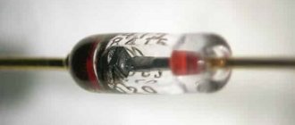
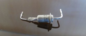
- The housing is a vacuum cylinder that can be made of glass, metal or durable ceramic varieties of material.
- inside the cylinder . The first is a heated cathode, which is designed to ensure the process of electron emission. The simplest cathode in design is a filament with a small diameter, which heats up during operation, but today indirectly heated electrodes are more common. They are cylinders made of metal and have a special active layer capable of emitting electrons.
- Inside the indirectly heated there is a specific element - a wire that glows under the influence of electric current, it is called a heater.
- The second electrode is the anode, it is needed to receive the electrons that were released by the cathode. To do this, it must have a potential that is positive relative to the second electrode. In most cases, the anode is also cylindrical.
- Both electrodes of vacuum devices are completely identical to the emitter and base of the semiconductor variety of elements.
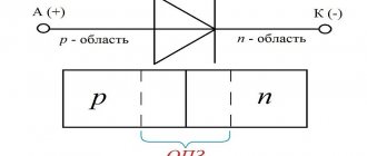
- Silicon or germanium is most often used to make a diode crystal One of its parts is p-type electrically conductive and has a deficiency of electrons, which is formed by an artificial method. The opposite side of the crystal also has conductivity, but it is n-type and has an excess of electrons. There is a boundary between the two regions, which is called a pn junction.
Such features of the internal structure give diodes their main property - the ability to conduct electric current in only one direction.
Purpose
Below are the main areas of application of diodes, from which their main purpose becomes clear:
- Diode bridges are 4, 6 or 12 diodes connected to each other, their number depends on the type of circuit, which can be single-phase, three-phase half-bridge or three-phase full-bridge. They perform the functions of rectifiers; this option is most often used in automobile generators, since the introduction of such bridges, as well as the use of brush-collector units with them, has made it possible to significantly reduce the size of this device and increase its reliability. If the connection is made in series and in one direction, this increases the minimum voltage required to unlock the entire diode bridge.
- Diode detectors are obtained by combining these devices with capacitors. This is necessary so that it is possible to isolate low-frequency modulation from various modulated signals, including the amplitude-modulated variety of the radio signal. Such detectors are part of the design of many household appliances, such as televisions or radios.
- Ensuring protection of consumers from incorrect polarity when switching on circuit inputs from occurring overloads or switches from breakdown by electromotive force that occurs during self-induction, which occurs when the inductive load is turned off. To ensure the safety of circuits from overloads that occur, a chain is used consisting of several diodes connected to the supply buses in the reverse direction. In this case, the input to which protection is provided must be connected to the middle of this chain. During normal operation of the circuit, all diodes are in a closed state, but if they have detected that the input potential has gone beyond the permissible voltage limits, one of the protective elements is activated. Due to this, this permissible potential is limited within the permissible supply voltage in combination with a direct drop in the voltage on the protective device.
- Switches based on diodes are used to switch high-frequency signals. Such a system is controlled using direct electric current, high-frequency separation and the supply of a control signal, which occurs due to inductance and capacitors.
- Creation of diode spark protection . Shunt-diode barriers are used, which provide safety by limiting the voltage in the corresponding electrical circuit. In combination with them, current-limiting resistors are used, which are necessary to limit the electric current passing through the network and increase the degree of protection.
The use of diodes in electronics today is very widespread, since virtually no modern type of electronic equipment can do without these elements.
Diode. Semiconductor diode. Diode connection. Diode marking. Diode operation.
| Basics |
A diode is an electronic device that allows current to flow in only one direction.
| Diode designation on diagrams |
A diode has two terminals called anode and cathode.
When a diode is connected to an electrical circuit, current flows from the anode to the cathode. The ability to conduct current only in one direction is the main property of a diode. Diodes belong to the class of semiconductors and are considered active electronic components (resistors and capacitors are passive).
| The triangle can be viewed as the tip of an arrow showing the direction of current |
When connecting a diode to a circuit, the correct polarity must be observed.
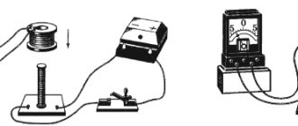
To make it easy to determine the location of the cathode and anode, special marks are applied to the body or one of the diode terminals. There are various ways to mark diodes, but most often a ring strip is applied to the side of the body corresponding to the cathode. If diode marking , then the terminals of semiconductor diodes can be determined using a measuring device - as mentioned above, the diode passes current only in one direction. If you don't have a measuring device at hand, you can use a battery and a low-power light bulb as described in the experiment below.
Diode operation
| Semiconductor diodes |
The operation of a diode can be visualized using a simple experiment.
If you connect a battery to a diode through a low-power incandescent lamp so that the positive terminal of the battery is connected to the anode, and the negative terminal to the cathode of the diode, then current will flow in the resulting electrical circuit and the lamp will light up. The maximum value of this current depends on the resistance of the semiconductor junction of the diode and the DC voltage applied to it. This state of the diode is called open, the current flowing through it is called direct current Ipr, and the voltage applied to it, due to which the diode is open, is called direct voltage Upr. If the leads of the diode are swapped, the lamp will not light up, since the diode will be in the closed state and provide strong resistance to the current in the circuit. It is worth noting that a small current will still flow through the semiconductor junction of the diode in the opposite direction, but in comparison with the forward current it will be so small that the light bulb will not even react. This current is called reverse current Irev, and the voltage that creates it is called reverse voltage Urev.
In the neural circuits of BEAM robots, diodes are often used to create neurons that model logical addition (OR gates). In addition, BEAM robot circuits sometimes make use of the capacitive properties of diodes.
Direct diode connection
The pn junction of the diode can be affected by voltage supplied from external sources. Indicators such as magnitude and polarity will affect its behavior and the electrical current conducted through it.
Below we consider in detail the option in which the positive pole is connected to the p-type region, and the negative pole to the n-type region. In this case, direct switching will occur:
- Under the influence of voltage from an external source, an electric field will be formed in the pn junction, and its direction will be opposite to the internal diffusion field.
- The field voltage will decrease significantly, which will cause a sharp narrowing of the blocking layer.
- Under the influence of these processes, a significant number of electrons will be able to freely move from the p-region to the n-region, as well as in the opposite direction.
- The drift current indicators during this process remain the same, since they directly depend only on the number of minority charged carriers located in the pn junction region.
- Electrons have an increased level of diffusion, which leads to the injection of minority carriers. In other words, in the n-region there will be an increase in the number of holes, and in the p-region an increased concentration of electrons will be recorded.
- The lack of equilibrium and an increased number of minority carriers causes them to go deep into the semiconductor and mix with its structure, which ultimately leads to the destruction of its electrical neutrality properties.
- In this case, the semiconductor
Diode circuits
to contents
Exercises
Methodical instructions Before this chapter, processes in linear circuits were considered. However, when analyzing circuits with real elements, in particular with diodes, it is necessary to take into account the nonlinearity of their characteristics, which is also reflected in the calculation method for such circuits. Let's consider the simplest methods for calculating nonlinear circuits used to solve the problems given in this and subsequent chapters. Current-voltage characteristic of a diode Analysis of the physical processes in the diode allows us to obtain an expression for its current-voltage characteristic in exponential form:
(9.10)
where Is is the saturation current, (rt is the thermal potential, Id Ud is the diode current and voltage across it, respectively. This is the simplest case of specifying the diode’s current-voltage characteristic in analytical form. You can measure the diode’s characteristics experimentally point by point, as was done in Section 9.1. Then the characteristic will be presented in tabular form. Finally, the current-voltage characteristic can be presented in graphical form, which is quite often used to present typical characteristics in reference data. The current-voltage characteristic of the diode is shown graphically in Fig. 9.21.
Graphical method This method is based on the direct use of the diode’s current-voltage characteristic, specified in graphical form. The graphical method is most suitable when there is only one diode in the circuit. Then the circuit can be divided into two parts: a linear non-ideal generator of voltage or current (active two-terminal network) and nonlinear (passive two-terminal network), and for the calculation use the equivalent generator method. The simplest scheme. In Fig. Figure 9.22 shows the simplest diagram for such an analysis. The current Id of the diode and the voltage Ud across it are related to each other by the following equations:
Equation (9.12) describes the diode’s current-voltage characteristic, which is given graphically in Fig. 9.22 (curve 1). Equation (9.11) reflects the load characteristic of a non-ideal EMF source, which is often called the load straight line (sloping line 2 in Fig. 9.22). The load straight line intersects the voltage axis at point A and cuts off on this axis the segment OA, numerically equal to the open circuit voltage of the power source E. The load straight line crosses the current axis at point B, cutting off on this axis the segment 0V, numerically equal to the maximum current E/R of the circuit. The current-voltage characteristic of the diode and the load straight line intersect at point C. This point is a solution to the system of equations (9.11), (9.12) in graphical form. The coordinates I*pr and U*np of point C are the desired current and voltage of the diode, respectively. The power source voltage can have any shape (for example, sinusoidal). The construction of a diode current time diagram for this case is shown in Fig. 9.23. For each moment of time (t1, t2, tз, etc.) it is necessary to find the instantaneous values of the power source voltage e(t) and construct the corresponding load straight line. The points of intersection of the load straight lines with the diode’s current-voltage characteristics determine the instantaneous values of the diode current for moments of time t1, t2, tз
When several diodes are connected in series, parallel or mixed in a circuit, they can be replaced by one nonlinear two-terminal network, after which the problem is reduced to the previous one. Let's consider this solution technique for various cases of connecting diodes. Series connection of diodes. Let two diodes be connected in series in the circuit, as shown in Fig. 9.24. The direct branches of the current-voltage characteristics of diodes VI, V2 are shown in Fig. 9.24 curves 1 and 2, respectively. Two diodes connected in series can be represented as one equivalent nonlinear two-terminal network, for example an equivalent diode. Since the voltage Unp on this equivalent diode is equal to the sum of the voltage Unp1 of diode VI and the voltage Unp2 of diode V2, to construct the I-V characteristics of the equivalent diode, it is necessary to add the I-V characteristics of the individual diodes (curves 1 and 2 in Fig. 9.24) by voltage. The result is curve 3 (Fig. 9.24). Now the task is reduced to the previous one. It is necessary to draw the load straight line AB and find its intersection with the current-voltage characteristic of the equivalent diode. These lines intersect at point C with coordinates I*pr and U*np. Knowing the current, you can use the I-V characteristics of the diodes to find the voltages U*np1 and U*np2. In the example considered, the diodes are biased in the forward direction. Let's consider the same circuit with reverse bias (Fig. 9.25). The reverse branches of the current-voltage characteristics of diodes VI, V2 are shown in Fig. 9.25 curves 1 and 2, respectively. By analogy with the case considered, it is necessary to add the voltage-voltage characteristics of the diodes. The result is curve 3 (Fig. 9.25). Point C of the intersection of the resulting current-voltage characteristic with the load straight line gives the reverse current of the diodes I*s and the reverse voltage i*s. The intersection with the characteristics of the diodes of a straight line parallel to the voltage axis and passing through point C gives the voltages on the diodes U*OBI and U*oB2. It should be noted that when the diodes are connected in series, the reverse voltages on them are not the same. The reason is that the reverse branches of the I-V characteristics of the diodes are not identical. To equalize the reverse voltages on the diodes, it is necessary to introduce additional elements into the circuit (for example, connect equalizing resistors in parallel with the diodes).
Parallel connection of diodes.
Let's consider a similar technique for parallel connection of diodes (Fig. 9.26). Two diodes connected in parallel can be considered as one equivalent nonlinear two-terminal network, for example an equivalent diode. Since the current 1pr of this equivalent diode is equal to the sum of the current Inp1 of diode VI and the current 1pr2 of diode V2, to construct the I-V characteristics of the equivalent diode, it is necessary to add the I-V characteristics of individual diodes (branches 1 and 2 in Fig. 9.26) by current. The result is curve 3 in Fig. 9.26. Now the problem has been reduced to the one solved earlier. It is necessary to draw the load straight line AB and find its intersection with the current-voltage characteristic of the equivalent diode. These lines intersect at point C. The result is a voltage U*np, which is the same for both diodes VI and V2. Knowing this voltage, you can use the I-V characteristics of the diodes to find the required currents I*np1 and I*pr2. It should be noted that when the diodes are connected in parallel, their currents are not the same. The reason for this is the non-identity of the direct branches of the I-V characteristics of the diodes. To equalize the currents, it is necessary to introduce additional elements into the circuit (for example, connect a equalizing resistor in series with each diode).
Graphic-analytical method
With the graphic-analytical method there are two stages of solution. The first is to approximate a graphically specified current-voltage characteristic by an analytical expression, the second is to solve systems of nonlinear equations compiled according to Kirchhoff’s laws using this expression. If, for example, in the system of equations (9.11), (9.12) we use (9.10) as the second equation, then the system will become transcendental and the solution cannot be obtained in analytical form. The most common type of approximation is linearization of the current-voltage characteristic. In this case, the diode is replaced by a model of simple linear elements. For the forward and reverse branches of the current-voltage characteristic, these models are different. In Fig. Figure 9.27 shows the direct branch of the diode’s current-voltage characteristic (line 1) and the segment of straight line 2 approximating this branch. The linear approximation equation has the form: Ud = Kdif.pr Id + Uo, (9.13) where Kdiff.pr is the differential resistance of the diode at forward bias, Uo - threshold voltage. To determine the value of Kdif. it is necessary to select two arbitrary points on the approximating straight line (line 2 in Fig. 9.27) (one of them may lie on the stress axis). For these points you need to find the voltage difference and current difference, and then divide the first difference by the second. This will be the desired value. A model of a forward biased diode, consisting of an ideal EMF source and resistance connected in series, is also shown in Fig. 9.27. In Fig. Figure 9.28 shows the reverse branch of the diode’s current-voltage characteristic (curve 1) and straight line segment 2 approximating this branch. The equation for such a linear approximation has the form:
(9.14)
where is Kdif. ov is the dynamic resistance of the diode at reverse bias, Io is the threshold current. The value of R differentials is determined in the same way as the value of R differential. etc. Next is the forward and reverse differential resistance of the diode RdiF. pr and R diF. We will denote OB
equally through Rdiff, distinguishing these designations only where necessary in the text. The current-voltage characteristic of the diode under reverse bias is described by expression (9.14). The same expression is valid for the two-terminal network shown in Fig. 9.28. Therefore, replacing the diode with a two-terminal one will be equivalent. Since the diode's current-voltage characteristic now has two different analytical expressions and two models (for the forward and reverse sections of the characteristic), it is necessary to determine which one to use. To do this, you must first find out in what state (direct or reverse) the diode is in the original circuit. In relatively simple circuits, the state of the diode is not in doubt. In more complex circuits, after completing the calculation, it is necessary to check the initial guess about the state of each of the diodes. If it was initially believed that the diode operates with forward (reverse) bias, and as a result of the calculation its current turned out to be negative (positive), then the assumption about the state of the diode is incorrect. It is necessary to use a different expression for the I-V characteristic of the diode (and a different model) and repeat the calculation. The resulting expressions (9.13) and (9.14) can be used to solve specific problems. If the forward voltage drop across an open diode is negligibly small compared to the voltages on other elements of the circuit, then the real forward branch 1 of the diode’s current-voltage characteristic in Fig. 9.21 can be replaced by a vertical straight segment 3. In this case, when calculating the circuit, we can assume that the diode leads (anode and cathode) are short-circuited. If the reverse current of a closed diode is negligible compared to the currents of other elements of the circuit, then the real reverse branch 2 of the diode’s current-voltage characteristic can be replaced by horizontal segment 4. In this case, when calculating the circuit, we can assume that the circuit with the diode is broken. It is clear that both ideal models are extreme special cases of linearization of characteristics. In this case, solving the problems is trivial, and such cases are not considered. The simplest circuit with one diode (Fig. 9.22), taking into account approximation (9.13), is described by the following system of equations:
Solving this system gives the expression for the diode current:
(9.17)
Series connection of diodes. A circuit with two diodes connected in series when connected directly (Fig. 9.24) is described by the system of equations:
where Rdiff.np1 Rdiff. at - differential resistances of diodes VI, V2 with forward bias, Uo1, Uo2 - threshold voltages of diodes VI, V2. The equivalent circuit corresponding to this case is shown in Fig. 9.29. The diode current is determined by the expression:
(9.21)
A circuit with two diodes connected in series under reverse bias (see Fig. 9.25), taking into account approximation (9.14), is described by the system of equations:
where Rdif.OBI, RDIF.OB2 are the differential resistances of diodes VI, V2 at reverse bias, lo1, Io2 are the threshold currents of diodes VI, V2. The equivalent circuit corresponding to this case is shown in Fig. 9.30. The diode current is determined by the expression:
(9.25)
The current Iob is negative because reverse voltage is applied to the diodes.
Parallel connection of diodes. The circuit with two parallel-connected diodes (see Fig. 9.26), taking into account approximation (9.13), is replaced by the circuit in Fig. 9.31 and is described by the system of equations:
The voltage on the diodes is determined using the nodal potential method by the expression:
(9.30)
The currents of diodes VI, V2 can be determined by substituting (9.30) into expressions for currents (9.28), (9.29). The feasibility of using one or another of the considered calculation methods is determined by the conditions of a specific task.
Calculation of circuits with one diode.
The circuits with one diode offered in the section (files c9_080...c9_111) contain a linear part with a complicated structure. To use the graphical method, you must first replace the linear part of the circuit with an equivalent generator. Let's consider the methodology for such a transformation. Let the circuit have only one nonlinear element, for example a diode. Let us select this diode from the entire circuit, as shown in Fig. 9.32a. The remaining linear part of the circuit can be represented as an equivalent active two-terminal network, which is shown in Fig. 9.326. This two-terminal network consists of two elements: an equivalent EMF source EEKV and an equivalent resistor REq (see section 2.1 regarding non-ideal voltage sources). The EEKV value can be easily measured in idle mode by connecting a voltmeter instead of a diode. The measured voltage is equal to the desired value Eq. To determine the value of Req, one could measure the short-circuit current of the two-terminal network, and then divide Eq by this current. This path is sometimes used to experimentally determine the parameters of an equivalent two-terminal network. When calculating Req, it is more convenient to take Eq = 0 and determine the resistance of the two-terminal network from its terminals. When determining the equivalent resistance, the terminals of the EMF sources in the original circuit must be short-circuited, and the branches with current sources must be opened. The same must be done in a real circuit when measuring resistance. In the measurement diagram shown on puc. 9.336, the terminals of the EMF source are short-circuited, and instead of a diode, a multimeter in ohmmeter mode is connected to the terminals of the two-terminal network. Calculation of circuits with several diodes. When calculating the circuits given in files c9_120...c9_137, it is necessary to replace the diodes with equivalent circuits. As a result of such a replacement, a linear design scheme will be obtained. Using methods for calculating linear circuits, you can determine the diode currents and voltages across them. After calculating the circuit, it is necessary to check the initial assumptions about the state of each of the diodes (forward or reverse bias). As a result of the calculation, it may turn out that the current of the diode replaced by an equivalent circuit for direct connection is negative. This means that initially an incorrect assumption was made about the direct connection of this diode. It is necessary to replace such a diode with its reverse bias equivalent circuit and repeat the entire calculation. The simplest option, a discontinuity, is used as an equivalent circuit for the reverse branch of the current-voltage characteristic in these problems. In experiments with models based on an ideal diode
reverse current is zero. Another case is also possible: the current of the diode, replaced by an equivalent circuit for reverse connection, turned out to be positive. This means that an incorrect assumption was made initially about the diode turning back on. It is necessary to replace the diode with its forward bias equivalent circuit and repeat the calculation.
Tasks for independent study Circuits with one diode Each of the tasks presented below (files c9_80... c9_87) contains a circuit with one diode. The current-voltage characteristic of this diode is shown in Fig. 9.34. Find the current and voltage of the diode using the graphical method and check the solution on Electronics Workbench. Similar problems с9_88...с9_111 are available on the floppy disk included with the book. If you don’t have a floppy disk, a complete list of problems included with the book can be found on the website of the DODECA publishing house (www.dodeca.ru).
Scheme options
Circuits with several diodes In the circuits presented in files c9_120...c9_137, find the currents and voltages of the diodes. The diode models shown in these circuits are obtained by adjusting the parameters of an ideal diode. In the designation of diodes shown in the diagrams, the numbers correspond to the parameters of the diode equivalent circuit with linear approximation (Fig. 9.27). The number following the symbol a indicates the diode resistance in Ohms, the number following it separated by a hyphen is the forward voltage drop in volts. For example, d5-0.7: Rdpr = 5 Ohm, Udpr = 0.7 V. Circuit options
to contents
Did you know,
that in 1965, two Americans Penzias (an emigrant from Germany) and Wilson declared that they had discovered cosmic radiation. A few years later they were given the Nobel Prize, as if no one knew the work of E. Regener, who measured the temperature of outer space by launching a bolometer into the stratosphere in 1933? Read more in the FAQ on ethereal physics.
Diode reverse connection
Now we will consider another method of switching on, during which the polarity of the external source from which the voltage is transmitted changes:
- The main difference from direct connection is that the created electric field will have a direction that completely coincides with the direction of the internal diffusion field. Accordingly, the barrier layer will no longer narrow, but, on the contrary, expand.
- The field located in the pn junction will have an accelerating effect on a number of minority charge carriers, for this reason, the drift current indicators will remain unchanged. It will determine the parameters of the resulting current that passes through the pn junction.
- As the reverse voltage , the electric current flowing through the junction will tend to reach its maximum. It has a special name - saturation current.
- In accordance with the exponential law , with a gradual increase in temperature, the saturation current indicators will also increase.
Forward and reverse voltage
The voltage that affects the diode is divided according to two criteria:
- Direct voltage is the one at which the diode opens and direct current begins to flow through it, while the resistance of the device is extremely low.
- Reverse voltage is one that has reverse polarity and ensures that the diode closes with reverse current passing through it. At the same time, the resistance indicators of the device begin to increase sharply and significantly.
The pn junction resistance is a constantly changing indicator, primarily influenced by the forward voltage applied directly to the diode. If the voltage increases, then the junction resistance will decrease proportionally.
This leads to an increase in the parameters of the forward current passing through the diode. When this device is closed, virtually the entire voltage is applied to it, for this reason the reverse current passing through the diode is insignificant, and the transition resistance reaches peak parameters.
Classification of diodes
Based on the source semiconductor material, diodes are divided into four groups:
- germanium,
- silicon,
- from gallium arsenide,
- from indium phosphide.
Germanium diodes are widely used in transistor receivers, as they have a higher transmission coefficient than silicon diodes .
This is due to their greater conductivity at a low voltage (about 0.1...0.2 V) of the high frequency signal at the detector input and a relatively low load resistance (5...30 kOhm).
According to their design and technological characteristics, diodes are distinguished:
- point,
- planar.
According to their purpose, semiconductor diodes are divided into the following main groups:
- rectifying,
- universal,
- impulse,
- varicaps,
- Zener diodes (reference diodes),
- stabilizers,
- tunnel diodes,
- reverse diodes,
- avalanche-span (ALD),
- thyristors,
- photodiodes, s
- LEDs and optocouplers.
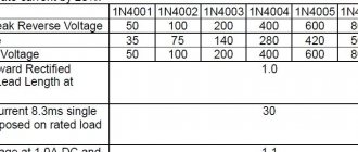
Diodes are characterized by the following basic electrical parameters :
- current passing through the diode in the forward direction (direct current Ipr);
- current passing through the diode in the opposite direction (reverse current Irev);
- the highest permissible rectified CURRENT Ivypr.max;
- the highest permissible direct current Ipr.add.;
- direct voltage Unp;
- reverse voltage IOBR;
- highest permissible reverse voltage iobr.max
- capacitance CD between the diode terminals;
- dimensions and operating temperature range.
Diode operation and its current-voltage characteristics
The current-voltage characteristic of these devices is understood as a curved line that shows the dependence of the electric current flowing through the pn junction on the volume and polarity of the voltage acting on it.
Such a graph can be described as follows:
- The axis is located vertically: the upper area corresponds to the forward current values, the lower area to the reverse current parameters.
- Horizontal axis: The area on the right is for forward voltage values; area on the left for reverse voltage parameters.
- The direct branch of the current-voltage characteristic reflects the passing electric current through the diode. It is directed upward and runs in close proximity to the vertical axis, since it represents the increase in forward electric current that occurs when the corresponding voltage increases.
- The second (reverse) branch corresponds to and displays the state of the closed electric current, which also passes through the device. Its position is such that it runs virtually parallel to the horizontal axis. The steeper this branch approaches the vertical, the higher the rectifying capabilities of a particular diode.
- According to the graph, it can be observed that after an increase in the forward voltage flowing through the pn junction, a slow increase in the electric current occurs. However, gradually, the curve reaches an area in which a jump is noticeable, after which an accelerated increase in its indicators occurs. This is due to the diode opening and conducting current at forward voltage. For devices made of germanium, this occurs at a voltage of 0.1V to 0.2V (maximum value 1V), and for silicon elements a higher value is required from 0.5V to 0.6V (maximum value 1.5V).
- The indicated increase in current readings can lead to overheating of semiconductor molecules. If the heat removal that occurs due to natural processes and the operation of radiators is less than the level of its release, then the structure of the molecules can be destroyed, and this process will be irreversible. For this reason, it is necessary to limit the forward current parameters to prevent overheating of the semiconductor material. To do this, special resistors are added to the circuit, connected in series with the diodes.
- By examining the reverse branch, you can notice that if the reverse voltage applied to the pn junction begins to increase, then the increase in current parameters is virtually unnoticeable. However, in cases where the voltage reaches parameters exceeding the permissible norms, a sudden jump in the reverse current may occur, which will overheat the semiconductor and contribute to the subsequent breakdown of the pn junction.
Diode design
Diodes are divided into several categories. They can be gas-discharge, electric vacuum and semiconductor, which are most widespread. Different diodes are used simultaneously in a single bundle, making it possible to convert alternating current to direct current. These properties are widely used in semiconductor and other devices.
The main structural elements of a semiconductor diode are plates made of specific semiconductor materials. Most often, germanium or silicon is used for this. On one side of the plate, p-type conductivity is observed, at which electrons are received. This conductivity is called hole conductivity. It is designed to fill the artificially created lack of electrons. The other side of the plate has n-type or electronic conductivity, in which excess electrons are given up.
Between both sides of the plate there is a layer called a pn junction. In all semiconductors, the p-type acts as the anode and the n-type serves as the cathode or negative electrode of the device.
Basic diode faults
Sometimes devices of this type fail, this may occur due to natural depreciation and aging of these elements or for other reasons.
In total, there are 3 main types of common faults:
- Breakdown of the junction leads to the fact that the diode, instead of a semiconductor device, becomes essentially a very ordinary conductor. In this state, it loses its basic properties and begins to pass electric current in absolutely any direction. Such a breakdown is easily detected using a standard multimeter, which starts beeping and shows a low resistance level in the diode.
- When a break occurs, the reverse process occurs - the device generally stops passing electric current in any direction, that is, it essentially becomes an insulator. To accurately determine a break, it is necessary to use testers with high-quality and serviceable probes, otherwise they can sometimes falsely diagnose this malfunction. In alloy semiconductor varieties, such a breakdown is extremely rare.
- Leakage , during which the tightness of the device body is broken, as a result of which it cannot function properly.
Breakdown of pn junction
Such breakdowns occur in situations where the reverse electric current begins to suddenly and sharply increase, this happens due to the fact that the voltage of the corresponding type reaches unacceptable high values.
There are usually several types:
- Thermal breakdowns , which are caused by a sharp increase in temperature and subsequent overheating.
- Electrical breakdowns that occur under the influence of current on a junction.
The graph of the current-voltage characteristic allows you to visually study these processes and the difference between them.
Electrical breakdown
The consequences caused by electrical breakdowns are not irreversible, since they do not destroy the crystal itself. Therefore, with a gradual decrease in voltage, it is possible to restore all the properties and operating parameters of the diode.
At the same time, breakdowns of this type are divided into two types:
- Tunneling breakdowns occur when high voltage passes through narrow junctions, which allows individual electrons to escape through it. They usually occur if semiconductor molecules contain a large number of different impurities. During such a breakdown, the reverse current begins to increase sharply and rapidly, and the corresponding voltage is at a low level.
- Avalanche types of breakdowns are possible due to the influence of strong fields that can accelerate charge carriers to the maximum level, due to which they knock out a number of valence electrons from atoms, which then fly into the conductive region. This phenomenon is avalanche-like in nature, which is why this type of breakdown received its name.
Thermal breakdown
The occurrence of such a breakdown can occur for two main reasons: insufficient heat removal and overheating of the pn junction, which occurs due to the flow of electric current through it at too high rates.
An increase in temperature in the transition and neighboring areas causes the following consequences:
- The growth of vibrations of the atoms that make up the crystal.
- entering the conductive band.
- A sharp increase in temperature.
- Destruction and deformation of the crystal structure.
- Complete failure and breakdown of the entire radio component.
Current-voltage characteristic of a semiconductor diode
The current-voltage characteristic of a semiconductor diode consists of a forward and reverse branch. They are located in the I and III quadrants, since the direction of current and voltage through the diode always coincides. Using the current-voltage characteristic, you can determine some parameters, and also clearly see what the characteristics of the device influence.
Conduction Threshold Voltage
If you apply direct voltage to the diode and begin to increase it, then at the first moment nothing will happen - the current will not increase. But at a certain value the diode will open and the current will increase according to the voltage. This voltage is called the conductivity threshold voltage and is marked on the current-voltage characteristic as Uthreshold. It depends on the material from which the diode is made. For the most common semiconductors, this parameter is:
- silicon – 0.6-0.8 V;
- germanium – 0.2-0.3 V;
- gallium arsenide – 1.5 V.
The property of germanium semiconductor devices to open at low voltage is used when working in low-voltage circuits and in other situations.
Maximum current through the diode when connected directly
After the diode opens, its current increases along with the forward voltage. For an ideal diode, this graph goes to infinity. In practice, this parameter is limited by the ability of the semiconductor device to dissipate heat. When a certain limit is reached, the diode will overheat and fail. To avoid this, manufacturers indicate the highest permissible current (Imax on the current-voltage characteristic). It can be approximately determined by the size of the diode and its housing. In descending order:
- Devices in a metal shell carry the greatest current;
- Plastic cases are designed for medium power;
- diodes in glass shells are used in low-current circuits.
Metal devices can be installed on radiators - this will increase the dissipation power.
Reverse leakage current
If you apply reverse voltage to the diode, the low-sensitive ammeter will not show anything. In fact, only an ideal diode does not allow any current to pass through. A real device will have a current, but it is very small, and is called the reverse leakage current (on the current-voltage characteristic - Irev). It is tens of microamps or tenths of milliamps and much less than direct current. You can determine it from the reference book.
Breakdown voltage
At a certain value of reverse voltage, a sharp increase in current occurs, called breakdown. It is tunnel or avalanche in nature and is reversible. This mode is used to stabilize voltage (avalanche) or to generate pulses (tunnel). With a further increase in voltage, the breakdown becomes thermal. This mode is irreversible and the diode fails.