Compensation voltage stabilizer
Compensating voltage stabilizer is a device in which stabilization is carried out due to the effect of changes in the output voltage on the regulator through a feedback circuit.
The most widely used are electromechanical (servo-drive, electrodynamic) compensation voltage stabilizers and step voltage correctors (discrete, key stabilizers). Compensating voltage stabilizers have a higher stabilization coefficient and lower output resistance compared to parametric ones. Their operating principle is based on the fact that a change in voltage across the load (under the influence of a change in Uin or In) is transmitted to a regulatory element (RE) specially introduced into the circuit, which prevents a change in voltage Un.
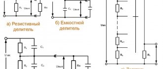
The regulating element (transistor) can be connected either in parallel with the load or in series with it. Depending
From this, two types of compensation voltage stabilizers are distinguished: parallel (Fig. 3.32, a) and series (Fig. 3.32, b).
The influence on the regulatory element in both types of stabilizers is carried out by a control circuit, which includes a direct current amplifier U and a reference voltage source ION. Using ION, the voltage across the load is compared with the reference voltage. The function of the amplifier is reduced to amplifying the difference between the compared voltages and supplying the amplified signal directly to the control element.
In the diagram of Fig. 3.32, and voltage stabilization at the load is achieved, as in a parametric stabilizer, by changing the voltage across the ballast resistor Rb by changing the current of the control element. If we take the input voltage of the stabilizer constant, then a constant voltage across the load will correspond to a constant voltage across the ballast resistor. A change in the load current from zero to Inmax will be accompanied by a corresponding change in the current of the control element from Inmax to zero.
In the diagram of Fig. 3.32, b the regulating element is connected in series with the load. Stabilization of the load voltage is carried out by changing the voltage on the regulating element. The current of the control element here is equal to the load current.
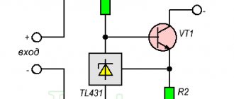
A schematic diagram of a series-type compensation voltage stabilizer is shown in Fig. 3.33, a. Transistor T1 serves as a regulating element, and the DC amplifier (single-stage) is made using transistor T2. The source of the reference voltage is a zener diode D connected to the emitter circuit of transistor T2. Resistor R (shown in dotted lines) is used to output the zener diode to the working section of the characteristic if the current IE2 of transistor T2 is small. Resistors R1, R2 are elements of the input voltage divider. The voltage between the base and emitter of transistor T2 Ube2=((R2/(R1+R2))*(Un-Uop).
The power circuit of the stabilizer, including the power source, transistor T1, and load Rн, is an amplification stage on transistor T1 with a common collector, in which Uin is the supply voltage, Ub1 is the input voltage, and Un is the output voltage (Un=Ub1-Ube1). To obtain the required voltage Un, it is necessary that the voltage at the output of the amplifier (Uк2=Uб1) be close to the voltage Un. To do this, the collector circuit of transistor T2 is powered from a separate source - Ek. The DC amplifier ensures that the required voltage Uк2 corresponds to the voltage of its input circuit Uв2. These considerations form the basis for the calculation of circuit elements based on the specified parameters Un, In of the nominal mode.
The stabilizing effect of the circuit is due to the presence in it of deep negative feedback on increments of the output voltage Un.
Let us assume that, under the influence of a decrease in voltage Uin, the voltage Un (hereinafter we mean absolute voltage values) has become less than the nominal value. A decrease in voltage Un causes a decrease in the voltage at the base Ub2 and the voltage Ube2 of transistor T2, and consequently, its currents Ib2 and Ik2. A decrease in current Ik2 leads to a smaller voltage drop across the resistor Rk and an increase in the voltages Ub1 and Ube1 of transistor T1. Due to an increase in voltage Ube1, the voltage Uke1 of transistor T1 decreases, thereby increasing the voltage Un to almost its previous value. Similar to what was considered, compensation is carried out for changes in voltage Un with an increase in Uin, as well as with changes in the load current.
The stabilization coefficient of the stabilizer is found from the relation
where rbx2, rb2, rk(e)2 are the input, base and collector resistances of transistor T2, respectively; A = 1 + rd/rin2+(R1? R2)/rin2?2 - correction factor that takes into account the influence of the dynamic resistance of the zener diode rd and the resistance of the divider in the base circuit of transistor T2.
Taking Ub1=const we have Rout=rе1+rb1/(1+?1), which is a fairly small value. Since the amplifier creates negative voltage feedback in the circuit, the output impedance is even lower. To calculate it, you can use the expression
The simplest compensation voltage stabilizer
So, the circuit of the simplest compensation voltage stabilizer is shown in the figure on the right.
Designations:
- IR - current through the ballast resistor (R0)
- Ist - current through the zener diode
- In — load current
- Iin - input current of the operational amplifier
- Id - current through resistor R2
- Uin - input voltage
- Uout - output voltage (voltage drop across the load)
- Ust - voltage drop across the zener diode
- Ud - voltage removed from the resistive divider (R1, R2)
- UОУ - output voltage of the operational amplifier
- Ube - voltage drop at the base-emitter pn junction of the transistor
Why is such a stabilizer called compensation and what are its advantages? In fact, such a stabilizer is a control system with negative voltage feedback, but for those who do not know what it is, we will start from afar.
As you remember, an operational amplifier amplifies the voltage difference between its inputs. The voltage at the non-inverting input is equal to the stabilization voltage of the zener diode (Ust). To the inverting input we supply part of the output voltage taken from the divider (Ud), that is, there we have an output voltage divided by a certain coefficient determined by resistors R1, R2. The difference between these voltages (Ust-Ud) is an error signal; it shows how much the voltage from the divider differs from the voltage on the zener diode (let’s denote this difference by the letter E).
Further, the output voltage of the op-amp is equal to E*Kou, where Kou is the gain of the operational amplifier with an open feedback loop (in the English literature Gopenloop). The voltage across the load is equal to the difference between the voltage at the op-amp output and the voltage drop at the base-emitter pn junction of the transistor.
Mathematically, everything we talked about above looks like this:
Uout=Uоу-Ube=E*Kоу-Ube (1)
E=Ust-Ud (2)
Let's take a closer look at the first equation and transform it to this form:
E=Uout / Kou + Ube / Kou
Now let's remember - what is the main feature of operational amplifiers and why everyone loves them so much? That's right, their main feature is a huge gain, of the order of 106 or more (for an ideal op-amp it is generally equal to infinity). What does this give us? As you can see, on the right side of the last equation, both terms have Coe in their divisor, and since Coe is very very large, therefore both of these terms are very very small (with an ideal op-amp, they tend to zero). That is, during operation, our circuit tends to a state where the error signal is zero. We can say that the operational amplifier compares the voltages at its inputs and if they differ (if there is an error), then the voltage at the output of the op-amp changes so that the voltage difference at its inputs becomes zero. In other words, he seeks to compensate for the error. Hence the name of the stabilizer - compensation.
Next, we have one more equation left. Given what we did with the first equation, the second equation will look like this:
0=Ust-Ud (2*)
Ud, as we remember, is part of the output voltage removed from the divider across resistors R1, R2. If we calculate our divider, not forgetting about the input current of the op-amp, we get:
and after substituting this expression into equation (2*), we can write the following formula (3) for the output voltage:
The input current of the operational amplifier is usually very small (micro, nano and even picoamps), therefore, with a sufficiently large current Id, we can assume that the current in both arms of the divider is the same and equal to Id, the rightmost term of formula (3) can be considered equal to zero, and rewrite formula (3) as follows:
Uout=Ust(R1+R2)/R2 (3*)
When calculating resistors R1, R2, it is necessary to remember that formula (3*) is valid only in the case when the current through the divider resistors is much greater than the input current of the operational amplifier. The value of Id can be estimated using the formulas:
Id=Ust/R2 or Id=Uout/(R1+R2).
Now let's evaluate the area of normal operation of our stabilizer, calculate R0 and think about what will affect the stability of the output voltage.
As can be seen from the last formula, only the stability of the reference voltage can have a significant impact on the stability of Uout. The reference voltage is the one to which we compare part of the output voltage, that is, it is the voltage across the zener diode. We will consider the resistance of the resistors to be independent of the current flowing through them (we do not consider temperature instability). The dependence of the output voltage on the voltage drop across the pn junction of the transistor (which is weak, but depends on the current), as in the case of a parametric stabilizer on a transistor, also disappears (remember when we calculated the error from the first formula - we divided the drop at the junction of the BE transistor by Coe and considered this expression equal to zero due to the very large gain of the op-amp).
From the above it follows that the main way to increase stability here is to increase the stability of the reference voltage source. To do this, you can either narrow the range of normal operation (reduce the input voltage range of the circuit, which will lead to a smaller change in the current through the zener diode), or take an integrated stabilizer instead of the zener diode. In addition, you can remember about our simplifications, then several more ways emerge: take an op-amp with a higher gain and lower input current (this will also make it possible to take divider resistors with a larger value - the efficiency will increase).
Okay, let's return to the area of normal operation and the calculation of R0. For normal operation of the circuit, the zener diode current must be in the range from Ist min to Ist max. The minimum zener diode current will be at the minimum input voltage, that is:
Uin min=IR*R0+Ust, where IR=Ist min+Iin
It’s similar here - if the zener diode current is much greater than the input current of the operational amplifier, then we can consider IR = Ist min. Then our formula will be written in the form Uin min=Ist min*R0+Ust (4) and from it we can express R0:
R0=(Uin min-Ust)/Ist min
Based on the fact that the maximum current through the zener diode will flow at the maximum input voltage, we will write another formula: Uin max=Ist max*R0+Ust (5) and combining it with formula (4) we find the normal operation area:
Well, as I already said, if the resulting input voltage range is wider than you need, you can narrow it, and the stability of the output voltage will increase (by increasing the stability of the reference voltage).
Parametric stabilizer
Its operating principle is based on the properties of semiconductor devices. The current-voltage characteristic of a semiconductor - a zener diode is shown in the graph.
During turn-on, the zener diode's properties are similar to those of a simple silicon-based diode. If the zener diode is turned on in the opposite direction, the electric current will initially increase slowly, but when a certain voltage value is reached, breakdown occurs. This is a mode where a small voltage increase creates a large zener diode current. The breakdown voltage is called stabilization voltage. To avoid failure of the zener diode, the current flow is limited by resistance. When the zener diode current fluctuates from the lowest to the highest value, the voltage does not change.
The diagram shows a voltage divider, which consists of a ballast resistor and a zener diode. A load is connected in parallel to it. When the supply voltage changes, the resistor current also changes. The zener diode takes over the changes: the current changes, but the voltage remains constant. When you change the load resistor, the current will change, but the voltage will remain constant.
An example of calculation and modeling of a compensating stabilizer
Initial data: — nominal output voltage of the stabilizer Uout – 11 V; — rated load current of the stabilizer Iout – 3 A;
— a source V1 of sufficient power is used, with an output voltage U1 = 2.5...3.5? Uout = 35 V.
— nominal load resistance RH = Uout / Iout = 3.67 Ohm.
Completing of the work:
1. Select the zener diode of the measuring bridge. Zener diode VD1 is selected with a stabilization voltage value Ust equal to half the output voltage Uout of the stabilizer:
Ust = Uout / 2 = 11 V / 2 = 5.5 V. The closest stabilization voltage is 1N4734, Ust = 5.6 V, Ist = 45 mA.
2. Find the resistor Rb: The voltage drops across the resistor:
URb = Uout – Ust = 11 V – 5.6 V = 4.4 V
Knowing the voltage drop and stabilization current, we determine the resistance of the resistor using Ohm’s law:
Rb = URb / = 4.4 V / 0.045 A = 98 Ohm
The closest resistor value in the nominal series is 100 Ohms. We find the resistor power from the condition PRb = URb? Ist ? K = 4.4 V ? 0.045A? 2 = 0.396 W, where K is the power reserve factor. The nearest highest resistor power value in the nominal series is 0.5 W. Thus, the parameters Rb are 100 Ohm; 0.5 W.
3. Let us determine the possible values of the output voltage of the stabilizer at which stabilization occurs. They are limited by the limiting currents of the zener diode located in the bridge measuring circuit. a) Let's determine the minimum (adjustable) stabilization voltage: According to the reference book, the minimum stabilization current 1N4734 Ist min = 0.2? Ist = 0.2? 45 mA = 9 mA, at this current the value of the output voltage of the stabilizer will be:
Uout min = Ust + (Ist min ? Rb) = 5.6 V + (0.009 A ? 100 Ohm) = 6.4 V
b) Let's determine the maximum (adjustable) stabilization voltage: According to the reference book, the maximum limit stabilization current 1N4734 Ist max reference = 162 mA. This is a large current at which the zener diode will operate in maximum mode and additional protection measures are needed, so we will limit ourselves to a value 2 times lower than the maximum stabilization current Ist max - 81 mA. At this current, the output voltage of the stabilizer will be:
Uout max = Ust + (Ist max ? Rb) = 5.6 V + (0.081 ? 100) = 17.75 V (hereinafter in calculations 18 V)
Since the power applied to the resistor has increased, in order for the resistor Rb not to fail due to high power dissipation, its power should be increased to the value:
PRb = I2st max? Rb ? 2 = 0.0812 A? 100 Ohm? 2 = 1.3322 W
The closest value is 2 W.
4. Let's calculate the divider R1, R2, R3: We know that the zener diode 1N4734 drops - 5.6 volts. In stabilization mode, transistor VT1 is at the “operating point,” which means that at its base-emitter junction the voltage “drops” by 0.65 volts. And this, in turn, means that there should always be 5.6 + 0.65 = 6.25 volts on the base relative to the stabilizer body. The base is connected to the “slider” of the middle adjustment resistor, which means that this voltage of 6.25 volts is always present on its “slider”. Based on this, it is possible to create a system of equations with three unknowns. At the maximum stabilization voltage Uout max = 18 V, the slider is in the lower position according to the diagram, the stabilization current Ist max = 81 mA, and the divider current R1, R2, R3 is 10 times less: Icircuit = 8.1 mA, therefore:
R3 = 6.25 V / I circuit = 6.25 V / 8.1 mA = 772 Ohm; R1 + R2 = (Uout max - UR3) / Icircuit = 18 V / 8.1 mA = 2222 Ohm.
Total resistance R1 + R2 + R3 = 720 + 2222 = 2942 Ohms. At a minimum stabilization voltage Uout min = 6.4 V, the divider current will be:
I circuit = Uout min / (R1 + R2 + R3) = 6.4 V / 2942 Ohm = 2.175 mA.
Let's find the value of R1 = (Uout min - 6.25) / Icircuit = (6.4 V - 6.25 V) / 2.175 mA = 69 Ohm, hence the value R2 = 2222 Ohm - 69 Ohm = 2153 Ohm, round the resistor values to values of the nominal series E24: R1 = 68 Ohm, R2 = 2.2 kOhm (variable), R3 = 750 Ohm
5. Let's calculate the second source of reference voltage and bias VT2. The rated stabilization voltage of zener diode VD2 is selected from the condition Ust2=3...4 Ust, where Ust is the rated stabilization voltage of zener diode VD1.
As a zener diode, we select a 1N4747 zener diode, the rated stabilization voltage of which is Ust2 = 22 V, Ist2 = 10 mA. Let's find Rcm. Rcm = (U1 - Ust2) / Ist2 = 35 - 22 / 10 mA = 1300 Ohm. Resistor power PRcm = (U1 - Ust2) ? Ist = 13 V? 10 mA = 0.013 W, the closest from the nominal range is 0.125 W. For stable operation of the reference voltage circuit Rcm VD2, it is necessary that Rk does not have a shunting effect on this circuit. Therefore, the current Rk must be at least 2 times less than the zener diode current. In addition, the difference between the input and output voltage drops on it: URк = U1 - Uout = 35 V - 11 V = 24 V,
hence: Rk = URk / (Ist2/2) = 24 V / 5 mA = 4800 Ohm.
Power РRк = URк ? Ist2 / 2 = 24 V? 5 mA = 0.12 W, nearest 0.125 W.
6. A 2N3501 transistor is suitable as VT1. It meets the requirements: - a sufficiently high gain (transmission) h21E = 100; - permissible collector-emitter voltage - 160 V,
— maximum collector current – 0.5 A.
A 2N3501 transistor is suitable as VT2. Transfer coefficient h21E = 100, which will ensure an increase in the resistor current Rk from 5 mA to 500 mA; For VT3 we select 2N6284. Transmission coefficient h21E VT3 = 750, maximum dissipation power – 160 W. With an output voltage = 11 V and a current of 3 A, the collector-emitter voltage VT3 should be 35 V -11 V = 24 V, thus the total power dissipation of the transistor will be: PVT3 = UVT3? I VT3 = 24 V ? 3 A = 72 W. 7.Re = (0.65 / Iout) ? h21E VT3 = (0.65 V / 3 A) ? 750 = 162.5 Ohms, where 0.65 V is the drop at the base-emitter junction, Iout is the rated load current = (3 amperes), h21E VT3 is the average value of the transistor transmission coefficient (750).
Select Re = 160 Ohm.
8. RH = Uout / Iout
Rice. 4.17. Scheme of a continuous compensation voltage stabilizer (example). Construct the amplitude (transfer) (example in Fig. 4.19) characteristic of the stabilizer. The initial source voltage V1 is 1 V, the final voltage V1 is 1.3? U1, the number of points is -100.
Rice. 4.18. View of the DC analysis settings windows.
By changing the voltage at the output of the stabilizer (with the slider of the variable resistor R6), set the output voltage Uout. Increase the voltage at the stabilizer input by +25%, measure Uout(Uin+25%), reduce the voltage at the stabilizer input by -25%, measure Uout(Uin-25%) and determine
ΔUout = Uout+25% – Uout-25%.
ΔUout = 11.0531 V – 11.0521 V = 1 mV
Rice. 4.19. View of the window with the amplitude (transfer) characteristic of the stabilizer. Determine the value of the stabilization coefficient:
Kst = (0.5? Uin) / (ΔUout/Uout),
Kst = (0.5?35V) / (1mV/11V) = 192519 Determine the efficiency of the stabilizer at various values of load resistance, according to Table 2:
Efficiency = Pout / Pin = (U1?Iin / Uout?Iout)100%
Table4.9
Measurement results. Dependence on load resistance
| Load resistance, R8, Ohm | 0.1RH | 0.5 RH | RH | 5 RH | 10RH | 100RH |
| U1, V | ||||||
| Iin, V | ||||||
| Uout, V | ||||||
| Iout, V | ||||||
| Pin, W | ||||||
| Pout, W | ||||||
| Efficiency, % |
Compensation stabilizer
The device discussed earlier is very simple in design, but makes it possible to connect power to the device with a current that does not exceed the maximum current of the zener diode. As a result, voltage stabilizing devices are used, which are called compensation devices. They consist of two types: parallel and serial.
The device is named according to the method of connection to the adjustment element. Compensating stabilizers of the sequential type are usually used. His diagram:
The control element is a transistor connected in series with the load. The output voltage is equal to the difference between the values of the zener diode and the emitter, which is several fractions of a volt, therefore it is considered that the output voltage is equal to the stabilizing voltage.
Parametric and compensation stabilizers. Protection of the voltage stabilizer from overloads.
There are two types of voltage stabilizers: parametric and compensation. The first type of stabilizers uses the constant voltage of certain types of devices when the current flowing through them changes (for example, a zener diode). In the second type of stabilizers, the problem of voltage stabilization is solved according to the compensation principle, based on automatic regulation of the voltage supplied to the load.
A semiconductor zener diode is a semiconductor diode, the voltage across which is maintained with a certain accuracy when current flows through it in a given range, designed to stabilize a constant voltage. The operating principle of the zener diode is based on the use of the electrical breakdown section on the reverse branch of the current-voltage characteristic of the pn junction.
The main parameters of the zener diode are: stabilization voltage Ust - the voltage drop across the zener diode when a given stabilization current flows; minimum Ist min and maximum Ist max currents of the zener diode; temperature coefficient of stabilization voltage,
differential resistance of the zener diode, determined in the breakdown section,
A device designed to stabilize DC voltage using a zener diode is called a parametric voltage stabilizer , since its characteristics are completely determined by the parameters of the zener diode.
High quality voltage stabilization can be obtained by using compensation stabilizers, which are
automatic regulators in which the actual output voltage
is compared with the reference (reference) voltage. The resulting mismatch signal is amplified and affects the regulator element of the stabilizer in such a way that the output voltage tends to reach the reference level. A parametric stabilizer operating with low load currents is usually used as a reference voltage source; less often, galvanic batteries are used.
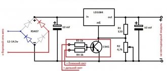
The role of the regulating element in this circuit is played by transistor VT1. As the input voltage Uin increases, the output voltage increases, creating a mismatch signal Ube at the input of the DC amplifier made on transistor VT2. The collector current of transistor VT2 increases, and its collector potential becomes more positive relative to ground. The base-emitter voltage of transistor VT1 decreases, which leads to an increase in the internal resistance of this transistor and a drop in voltage across it. The output voltage decreases, tending to its previous value. To obtain the reference voltage Uop, a parametric voltage stabilizer is used, consisting of a resistor Rb and a zener diode VD1.
Stabilizers on microcircuits
Such devices in the integrated version have increased characteristics of parameters and properties that differ from similar semiconductor devices. They also have increased reliability, small dimensions and weight, as well as low cost.
Series regulator
- 1 – voltage source;
- 2 – Adjustment element;
- 3 – amplifier;
- 4 – main voltage source;
- 5 – output voltage detector;
- 6 – load resistance.
The adjustment element acts as a variable resistance connected in series with the load. When the voltage fluctuates, the resistance of the adjustment element changes so that compensation for such fluctuations occurs. The control element is influenced by feedback, which contains a control element, a main voltage source and a voltage meter. This meter is a potentiometer from which part of the output voltage comes.
The feedback adjusts the output voltage used for the load, the output voltage of the potentiometer becomes equal to the main voltage. Voltage fluctuations from the main one creates some voltage drop at the regulation. As a result, the output voltage can be adjusted within certain limits by the measuring element. If the stabilizer is planned to be manufactured for a certain voltage value, then the measuring element is created inside the microcircuit with temperature compensation. If there is a large output voltage range, the measuring element is performed behind the microcircuit.
Parallel stabilizer
- 1 – voltage source;
- 2 – regulating element;
- 3 – amplifier;
- 4 – main voltage source;
- 5 – measuring element;
- 6 – load resistance.
If we compare the circuits of stabilizers, then a device of a sequential type has increased efficiency at partial load. A parallel type device consumes constant power from the source and supplies it to the control element and the load. Parallel stabilizers are recommended for use with constant loads at full load. The parallel stabilizer does not create a danger in the event of a short circuit, the sequential type does not create a danger during idle. At a constant load, both devices create high efficiency.
Relay voltage stabilizer
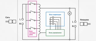
Stabilizers with step relay switching have an autotransformer (AT) winding with many taps. Each winding tap corresponds to different transformation ratios. The electronic circuit of the control unit (CU), analyzing the state of the network, switches power relays (R) connected to different sections of the autotransformer winding, providing a stable output voltage.
Advantages of this type of stabilizer:
- relatively cheap solution - there are no expensive and difficult to manufacture elements;
- wide range of operating voltages - the lower limit of the input voltage is most often 140V, but there are models for 125, 110 and even 90V. the upper limit is usually 270V-280V. At a lower or higher input voltage, the stabilizer will simply disconnect the load from the network;
- high efficiency - losses only on the transformer (efficiency >95%) and a little on the control unit and relay heating;
- high performance is one of the main advantages of this type. When there is a sharp change in the input voltage, the stabilizer does not go through all the relays in turn, but immediately switches to the one needed. Response time is typically 20ms;
- the correct sine wave at the output - this is in comparison with inverter stabilizers which introduce significant distortion into the sine wave of the output voltage - consumer devices do not like this.
Flaws:
- protects only from low or high voltage;
- stepwise adjustment of the output voltage - there’s no escape from this technology. Typically the voltage difference between pins is 4-10%;
- The low switching life of power relays is the main problem with this type of stabilizer. Relays do not like overloads very much and with frequent switching they quickly fail;
- maximum power usually up to 12 kVA
- noise when switching the relay - yes, the clicks are heard very well, besides, like any representative of transformer devices, the autotransformer hums.
- low resistance to polluted environment and moisture - the autotransformer needs cooling under heavy loads - therefore, any stabilizer has a lot of ventilation holes. At the same time, there are models with forced ventilation, and like a vacuum cleaner, they draw a lot of dust into the case, which penetrates the power relays (especially on powerful models), which quickly damages them.
Let's move on to the second type of stabilizers
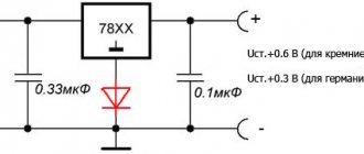
Stabilizer on a chip with 3 pins
Innovative variants of sequential stabilizer circuits are made on a 3-pin microcircuit. Due to the fact that there are only three outputs, they are easier to use in practical applications, since they displace other types of stabilizers in the range of 0.1-3 amperes.
- Uin – raw input voltage;
- U out – output voltage.
You may not use containers C1 and C2, but they allow you to optimize the properties of the stabilizer. Capacity C1 is used to create system stability, capacitance C2 is needed for the reason that a sudden increase in load cannot be tracked by the stabilizer. In this case, the current is supported by capacitance C2. In practice, 7900 series microcircuits from Motorola are often used, which stabilize a positive voltage value, and 7900 – a value with a minus sign.
The microcircuit looks like:
To increase reliability and create cooling, the stabilizer is mounted on a radiator.
Main types of voltage stabilizers
The growing demand for voltage stabilizers is associated both with the active use of these electrical appliances in all spheres of human activity, and with problems with the quality of electricity that periodically arise in networks.
Specialized stores and online sites offer a large selection of stabilizers of domestic and foreign production, satisfying almost any customer needs.
Each stabilizer, despite its power and cost, is built according to a standard circuit (topology), which is based on a certain physical principle of stabilizing electrical energy. There are five such topologies in total:
- ferroresonant;
- electromechanical;
- relay;
- semiconductor;
- inverter
Almost all types of voltage stabilizers have their advantages and disadvantages, which are mainly determined by the design of their construction. The main parameters of devices of each type require careful study, since the efficiency of the selected stabilizer model with various modern equipment depends on their values.
