Parsing the circuit
This is a mono audio power amplifier.
Transistor VT1 is the main element in the amplifier circuit. Therefore, the circuit is called a transistor ULF (low frequency amplifier).
In this case, an NPN transistor is used. It is connected according to a common emitter (CE) circuit. This circuit allows you to get the most out of the transistor. It amplifies both voltage and current at the same time. Total maximum power.
How exactly is the switching scheme determined? The incoming signal is fed to the base and emitter, and the output signal is taken from the collector and emitter. That is, in fact, a common emitter contact. That's why the circuit is called common emitter. The emitter is the power part of the transistor, which allows you to amplify the signal to the maximum.
This circuit has one amplification stage.
What is a cascade
A cascade is essentially an amplification stage that is independent of the other. There are also two-stage amplifiers. That is, for example, there are two transistors in the circuit. One works as a preamplifier and transmits the amplified signal to the input of the second. Therefore, the circuit is called two-stage. They are independent of each other, but the first stage transmits the signal to the second, which allows the signal power to be increased.
Simple audio amplifier circuit
Any low-frequency stage intended for music reproduction consists of a preliminary block, tone controls or equalizer, and a final stage. If the device is intended to work with multiple audio sources, an input selector should be provided. Since the signal level from different devices differs from each other, the selector takes into account the possibility of equalizing the input voltages through amplification or limitation. The most sensitive is the microphone input, and the “roughest” is the input intended for connecting the linear output of a radio or tuner. The circuit diagram of the preliminary stage can be assembled using transistors or operational amplifiers.
A simple audio amplifier circuit with sound controls and tone controls is implemented on a single reverse conduction transistor. In the circuit it is recommended to use KT315 or KT3102 with any letter index. Resistor R8, on the collector of the transistor, sets the voltage to 6 volts, and resistor R1 can be replaced with a constant one. Its value is selected depending on the input signal level.
It is easy to assemble an audio amplifier circuit with your own hands using an operational amplifier, which has a high input impedance, a wide processing bandwidth and a low level of intrinsic noise.
This circuit uses the K1401UD2 microcircuit, which contains 4 separate nodes with a common power supply. This chip assembles the preliminary channel for the stereophonic path. 2 op-amps operate in the right channel and 2 in the left. In the monophonic version, only two elements can be used. The device consists of a pre-level increase channel with input voltage correction and an active three-band tone control that operates at low, mid and high frequencies. A significant disadvantage of preliminary stages on operational circuits is that they require a bipolar power supply, which significantly complicates the design.
The sound power amplifier can also be made on a different element base. Most often, complementary pairs of transistors of different conductivities or specialized integrated circuits are used for this purpose. A simple cascade is assembled using low-power silicon transistors. Instead of the KT315-KT361 pair, you can use the KT3102-KT3107 pair.
Before applying power, the speaker should be turned off, and instead of resistor R1, install a chain of a 33 kOhm constant resistor and a 270 kOhm potentiometer connected in series. Turn on the power and rotate the potentiometer to set the specified collector current at the control point. Then measure the resulting resistance of the chain and replace it with the closest nominal constant resistor. Next, by selecting resistor R3, you need to set half the supply voltage at the same point. Next, a speaker is connected and a low-frequency signal from the sound source is supplied to the input. The circuit does not have a volume or tone control, so any pre-stage that has these functions can be connected to it.
How to eat scheme
The quality of the amplification also depends on the quality of the power supply. No matter how outstanding the characteristics of the transistor, if the power supply is poorly filtered or insufficient, then the amplification will be of advisable quality.
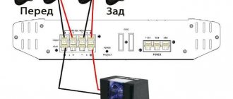
6 V power is connected to terminals X3 and X4.
This circuit can also be powered by a battery. However, despite the fact that the battery is a source with minimal noise, the battery also has its own resistance.
And so that it does not interfere or affect the operation of the amplifier, a smoothing and storage capacitor is needed.
Electrolytic capacitor C3 stores energy from the power supply, which improves the quality of amplification. The higher the capacity, the better. Naturally, this rule has limitations. If you install too large a container, there will be a large load on the power supply.
In addition, electrolytic capacitors must discharge after switching off. Moreover, there is a limit to increasing the capacity for the circuit. If a capacitor with a capacity of 1 farad (1,000,000 μF) is connected to this circuit, then the noise level at the amplifier output will be the same as at 1000 μF. This is due to the fact that the transistor also has its own “noise”, lack of shielding at the input, dynamic distortion and other parameters.
During circuit design, all these parameters are calculated. Here in the circuit, capacitor C3 has a capacity of 47 microfarads - this is enough for our transistor, since it does not have much power that it can produce. You can also supply a larger capacity, for example, 1000 microfarads. The main thing is not to carefully install a capacitor with a lower voltage limit. If you put a capacitor less than 6 V (power supply to the circuit), the capacitor will start to heat up and may even explode.
Basics of electroacoustics
Electrical signal amplifiers are electronic devices designed to amplify the voltage, current, or power of input electrical signals using energy from a power source. In Fig. 10.1 shows the transmission of a signal using an amplifier to a load, while the power in the load is P2
greater than the power of the input signal
P1
and changes over time according to a law similar to the law of change
P1
.
Note that any energy conversion is accompanied by losses, which lead to heating of the amplifier elements and are taken into account in the form of power dissipation P
r.
Fig. 10.1. Signal transmission using an amplifier
The essence of the signal amplification process is to convert the energy of the amplifier's power source into the energy of the output signal according to the law determined by the input control action, i.e. any amplifier modulates the energy of the power supply with an input control action. This process is carried out using a managed element. These elements in modern amplifiers are made, as a rule, using bipolar or field-effect transistors.
Classification of amplifiers . All amplifiers can be classified according to the following criteria.
According to the type of signal being amplified, amplifiers are divided into
- DC amplifiers (DCA), amplifying electrical signals with a frequency of zero hertz and higher
- AC amplifiers that amplify alternating signals with a frequency other than zero.
Based on the frequency of the amplified signal, the following groups can be distinguished:
- low frequency amplifiers (LF) - devices with a range of amplified frequencies from a few hertz to hundreds of kilohertz;
- high frequency amplifiers (UHF) - devices with a range of amplified frequencies from hundreds of kilohertz to hundreds of megahertz and higher;
- broadband amplifiers (WPA) – devices with a range of amplified frequencies from tens – hundreds of hertz to hundreds of megahertz;
- selective (resonant) amplifiers (AM), providing amplification in a narrow frequency range.
Fig. 10.2. Frequency response: a) UPT, b) ULF, c) UHF, d) silo, e) IU
Based on the type of signal being amplified, they are divided into
amplifiers
- harmonic signals.
- pulse signals.
Amplifiers of harmonic signals are designed to amplify signals whose changes occur much slower than the duration of transient processes in the amplifiers themselves.
Pulse signal amplifiers are designed for pulsed periodic and non-periodic signals. In this case, the duration of the intrinsic transient processes in the amplifier should not cause distortion of the original shape of the amplified signals.
According to their functional purpose they are divided into
- voltage amplifiers,
- current amplifiers
- power amplifiers
depending on which parameter needs to be enhanced.
According to the type of connecting circuits of the amplifier stages. Since amplifiers are built, as a rule, based on the sequential connection of several standard stages, amplifiers with
- galvanic (direct) connection, providing for the transmission of both alternating and direct current signals between signal stages; amplifiers with RC
connections, in which a resistive-capacitive coupling is included between the output of the previous and the input of the subsequent stages, eliminating the transmission of direct current signals; - amplifiers with inductive (transformer) coupling, in which a transformer is connected between the stages.
Amplifier input
The amplifier input is terminals X1 and X2.
X2 is the minus of the input, and X1 is the plus. Since the circuit is for one channel, the ULF is called mono.
You can connect both the left and right channels, or both at once.
Input filtering
Electrolytic capacitor C1 allows you to separate the DC component of the incoming signal from the variable one.
Simply put, it only passes the AC signal. If there is no signal, or the amplifier input is short-circuited, then without this capacitor the transistor may go into saturation mode (maximum gain), and an unpleasant wheeze will appear at the output.
Do not confuse this effect with whistling. The whistle is the influence of positive feedback, and in this case there will be a saturation mode due to a short circuit at the input. And at the output of the amplifier, it is the wheezing that will be heard, and not the sound or sound.
The capacitance of the capacitor is matched to the frequency of the sound signal. The sound starts from 20 Hz and up to 16 kHz.
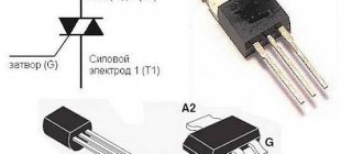
Bipolar transistor power amplifier
Amplifiers with bipolar transistors are formed using three connection schemes:
- OB – common base (characteristic: voltage gain, current constant, low resistance at the input and high at the output);
- OE - common emitter (characteristic: amplification of voltage, current and power, average readings for input and output resistance in comparison with OB and OK);
- OK - common collector (characteristic: increased current, constant voltage, high resistance at the input and low at the output).
OE is the most common connection option.
The characteristics of transistors change greatly when exposed to different temperature conditions. The same applies to simple amplifiers with OE. Therefore, the operation of the circuit is usually corrected using emitter and collector stabilization.
However, collector stabilization is fraught with a decrease in the signal gain, and therefore the efficiency of the device. A decoupling capacitor can help prevent this by eliminating negative AC feedback.
But still, emitter stabilization is used much more often.
In one of the articles in Radio magazine, V. Grechishkin proposed a drawing of a printed circuit board for an amplifier using bipolar transistors. According to him, this circuit provides a rated power level of up to 70 watts with a resistance of 4 ohms. If you increase the power to 8 ohms, then the power increases to 40 watts. Changes in the amplitude-frequency response in the range from 20 to 20,000 Hertz are ±0.5 dB. With a closed background, the background and noise voltage does not exceed 1 mV.
This is an incomplete description, but it is also quite attractive for a knowledgeable radio amateur. Therefore, it makes sense to study this article with the accompanying diagram.
Write comments, additions to the article, maybe I missed something. Take a look at the site map, I will be glad if you find anything else useful on my site.
Operating point and base offset
To ensure that the transistor does not distort the input signal, you first need to open it slightly.
This can be done using a voltage divider consisting of two resistors R1 and R2. This voltage divider allows you to slightly open the transistor VT1 so that the input signal does not waste its electrical energy on its opening.
The current that flows through R1 and R2 goes to the base of transistor VT1, which then goes through the emitter, thereby opening it. This is called the base bias of the transistor, that is, its opening. The bias voltage determines the operating point. In this case, a class A amplifier.
How is the amplifier class determined?
The class of an amplifier is determined by its operating point. The operating point is selected using the current-voltage characteristic of the transistor. The higher the voltage applied to the transistor input, the greater the current, the higher the operating point.
For example, the point in the center is class A.
And the class is the highest quality of amplifiers. It amplifies both the positive and negative half-waves of the input signal. At the same time, this class has a significant drawback. This limits power and reduces energy efficiency. The fact is that as long as no input signal is received at the ULF input, it works all the time while it is turned on.
It turns out that this wastes excess electricity. Therefore, the operating point is also called the resting point, when the amplifier does not amplify the input signal.
The sensitivity of the amplifier also depends on the operating point.
There are also class B, AB and D. They differ from each other in amplification efficiency and the presence of distortion. It all depends on the scheme used.
For example. Class D does not open the transistor at all, but from the point of view of energy efficiency it is the best choice. The transistor does not consume anything at rest; it turns on only when an input signal is applied. And at the same time, if an analog audio signal is supplied to the input, it is distorted. Such a class will not be suitable for the scheme that we are analyzing in this article.
Therefore, circuit designers and engineers invented digital amplifiers. Their analog signal is converted to digital, and only then fed to the input of the amplifier. The transistor does not distort the signal with the input digit. After amplification, the signal is again converted to analog with the least loss and distortion.
And the AB mode is used in circuits where there are several transistors that operate at their own half-waves. There are circuits where one transistor amplifies only positive half-waves, and the second only negative ones. Such amplifiers are called push-pull.
Power Amplifiers: Definition, Circuits, Powerful Output Amplifiers
A power amplifier is an amplifier designed to provide a given load power РН at a given load resistance RH.
A power amplifier is an example of power electronics devices. The main goal in developing such devices is to deliver a given power to the load. In contrast to power electronics devices, when designing data electronics devices, the main goal is to perform specified signal processing and obtain output signals containing some information about the input signals.
Vasiliev Dmitry Petrovich
Professor of Electrical Engineering, St. Petersburg State Polytechnic University
Ask a Question
As an example, we can name devices that determine at what point in time the input signal takes on its maximum value. In information electronics devices, as a rule, they strive to reduce the power of the processed signals to a level at which the noise immunity of the device is still acceptable. In power electronics devices, such a task, in accordance with the above, cannot be posed in principle.
A real device may contain features of both power and data electronics, but this distinction should be kept in mind. It should be noted that the functions of information electronics devices are increasingly being taken over by microprocessors. But microprocessors, naturally, are not able to perform the functions of power electronics devices.
The power amplifier, as a rule, accounts for the vast majority of the power consumed by the device of which it is an integral part. Therefore, every attention is paid to increasing the efficiency of the power amplifier.
Another important issue is reducing the overall dimensions and weight of the power amplifier, since they often determine the overall dimensions and weight of the entire device. The problems of increasing efficiency and reducing overall dimensions are closely related, because the overall dimensions and weight of the amplifier are highly dependent on the overall dimensions and weight of the coolers. The higher the efficiency, the smaller the overall dimensions and weight of the amplifier.
Abrahamyan Evgeniy Pavlovich
Associate Professor, Department of Electrical Engineering, St. Petersburg State Polytechnic University
Ask a Question
Power amplifier transistors operate in large signal mode, when the amplitudes of the alternating current and voltage components are sufficiently large. In this case, the nonlinear properties of the transistors noticeably manifest themselves and nonlinear distortions of the input signal occur. On the other hand, it is usually not allowed for the output signal to be highly distorted.
The level of nonlinear distortion and the efficiency of the power amplifier significantly depend on the initial operating mode, and nonlinear distortion is caused by the nonlinearity of not only the input but also the output characteristics of the transistors, since they operate in large signal mode. The minimum possible level of nonlinear distortion can be achieved in class “A” mode, and the highest possible efficiency - in class “B” or “AB” mode.
Power amplifiers are single-cycle and push-pull, with the former operating in class “A” mode, and the latter in class “B” or “AB” mode. Single-ended power amplifiers are used at relatively low output powers (several watts).
In accordance with the requirement to provide a given load power Pn, when developing a power amplifier, the question of the appropriate choice of the amplifier supply voltage E must be resolved. Let us assume that an amplifier with the specified supply voltage can create a sinusoidal signal with the maximum possible voltage amplitude at the load
Then the maximum possible load power Pn max is determined by the expression Pn max = (Um / √2)2 1 / Rn = Um2 / (2 Rn) = E2 / (8 Rn)
From where Um = E / 2 E = 2 √ (Рн max · Rн 2 )
If for some reason it is not possible to select the obtained value of E, a transformer can be used to match the amplifier and load. However, a transformer is often an undesirable element of a power amplifier, as it is a relatively expensive and difficult device to manufacture.
Let's consider matching the load and amplifier using a transformer (Fig. 2.39).
W1 and W2 indicate the number of turns of the primary and secondary windings of the transformer, respectively, and uout and Rout indicate the output voltage and output resistance of the amplifier, respectively.
When determining the load power, this circuit can be replaced by the equivalent circuit shown in Fig. 2.40.
In it, R′н denotes the reduced load resistance R′н = Rн / n 2 where n is the transformation ratio (n = W2 / W1).
By changing the transformation ratio, it is possible to achieve the necessary coordination between the amplifier and the load, and it is known that the maximum power is delivered to the load at Rout = R′n. From here we determine the optimal value of the transformation ratio:
n opt = √ ( Rн / Rout )
Stabilization of the circuit operation
When a semiconductor heats up, its resistance decreases. The transistor is made of a semiconductor, and accordingly its pn junctions are too.
When the ULF circuit operates, current flows through the transistor and it heats up. Typically all power is dissipated at the collector. Nevertheless, the characteristics of the transistor change dramatically, since the resistance of its pn junction decreases sharply as the temperature rises.
To stabilize the operation of the transistor, you need to balance its resistance with another source. This can be done using additional resistance.
When the resistance of transistor VT1 decreases, resistor R3 takes part of the voltage onto itself and does not allow the current in the circuit to increase.
Thanks to this, the transistor:
- does not close;
- does not go into saturation mode;
- does not distort the signal;
- and doesn't overheat.
This is called thermal stabilization of the amplifier.
And so that in normal operation, when VT1 does not heat up, resistor R3 does not reduce the power of the circuit, a shunt electrolytic capacitor C2 is included in the circuit. The variable component of the input signal passes through it without loss.
Principle of operation
From the very designation of class AB, it is easy to conclude that this mode is a hybrid of class A and class B. We have already figured out how class A amplifiers work, but we did not have time to familiarize ourselves with class B, so we will start with it. And to begin with, let us remember the logic that guided the creator of the class A amplifier. In order to be able to reproduce both positive and negative half-waves using one active element, he applied a shift of the midpoint (quiescent current) to the middle of the working area of the lamp.
The creators of Class B amplifiers reasoned differently: “If one tube or one zero-bias transistor can reproduce only one half-wave of the signal, why not add another active element to the circuit, placing it in a mirror, to reproduce the other half-wave?”
This is quite logical, because in this situation both transistors operate with zero bias. As long as there is a positive half-wave at the input of the amplifier, one transistor works, and when the time comes to reproduce the negative half-wave, the first transistor is completely closed and the second one switches on instead. In the English version, this operating principle is called push-pull or, in Russian, “pull-push,” which in general describes what is happening very well.
When comparing Class B to Class A, the most obvious advantage is that in Class B, each wavelength covers the full operating range of the transistor (or tube), while in Class A, both half-waves are reproduced by a single active element. This means that a class B amplifier will be twice as powerful as a class A amplifier assembled using the same transistors.
The second, slightly less obvious, but very important advantage of class B is zero bias currents. When the input signal is zero, the current flowing through the transistors is also zero, which means that there is no wasted energy consumption, and the energy efficiency of the circuit is several times higher than in class A.
However, the main drawback of a class B amplifier follows from this same fact. The moment the transistor is turned on after a completely closed state is accompanied by a slight delay, therefore, when the sound signal passes the zero point, when one transistor has already closed, the second transistor does not have time to instantly pick up the baton, and in At this very transition point, small time delays occur.
In practice, this is expressed in the amplifier’s particular dislike for quiet music, as well as in poor transmission of microdynamics. And although history knows successful implementations of class B, for example, the legendary Quad 405, the problems of this operating mode have not gone away. The same 405 not only pleased with its energetic and muscular sound, but also had a clear tendency to paint a sound picture with large strokes, on a large scale, without wasting time on trifles.
In order to preserve all the advantages of class B and solve the problem of transient processes, the engineers resorted to a trick. They turned on both transistors with a bias, as is done in class A, but the bias value was chosen to be significantly smaller: so as to cover only those moments when the transistor is close to closing, thereby removing transient processes from the working area.
This allowed the class AB amplifier to quietly overcome the zero point, and also provided another extremely useful effect. When the signal amplitude is small, falling within the limits of the quiescent current bias, such an amplifier operates in class A and only when the amplitude goes beyond the bias value selected by the manufacturer does it switch to AB mode.
Amplifier output
At the output of the amplifier, you can connect either another amplifier, which will amplify the signal even more, or a dynamic head. The dynamic head is a regular speaker. It will reproduce the sound from the output of transistor VT1.
However, there are many nuances here too.
The most important thing concerns the matching of the load resistance and the amplifier resistance.
If the output resistance of the transistor is much greater than that of the dynamic head, then it will not be able to transmit all the power. At a minimum, most of the voltage will remain on its contacts.
This circuit requires a speaker with a resistance of about 1 kOhm.
If you set it less, for example, by 4 Ohms, then even half the power will not be reproduced, and the VT1 collector will begin to heat up even more.
The matching of the input, output and amplifier load resistances is calculated at the circuit design stage. Therefore, they should not be violated.
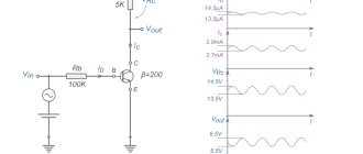
How does current flow through the circuit?
At the initial moment of time, when the power is connected, the electrolytic capacitor C3 is charged, and the collector and emitter of the transistor VT1 begin to be powered. And also the current passes through the voltage divider.
The voltage divider R1, R2 biases the base of VT1. The base-emitter bias current (B-E) begins to flow, thereby establishing the ULF operating point.
When the input signal arrives at terminal X1, it passes through C1 and through the divider enters the base of VT1 and partially leaves through the emitter.
The input signal is attracted by the collector VT1 and thereby amplified.
That part of the alternating signal that has passed to the emitter of the transistor is amplified by the emitter current. It passes freely through C2, which, paired with R3, stabilizes the amplifier’s operating mode from overheating and distortion. As a result, the input signal, amplified by the collector-emitter (C-E) current VT1, is sent to the output, that is, to the dynamic head BF1.
Electrical signal amplifiers. Varieties, parameters. Characteristics.
Electrical signal amplifiers are electronic devices designed to amplify the voltage, current, or power of input electrical signals using energy from a power source.
Signal transmission using an amplifier.
All amplifiers can be classified according to the following criteria.
Based on the type of signal being amplified, amplifiers are divided into direct current amplifiers (DCA), which amplify electrical signals with a frequency of zero hertz and higher, and AC amplifiers, which amplify alternating signals with a frequency other than zero.
Based on the frequency of the amplified signal, the following groups can be distinguished: low frequency amplifiers (LF) - devices with a range of amplified frequencies from a few hertz to hundreds of kilohertz;
high frequency amplifiers (UHF) - devices with a range of amplified frequencies from hundreds of kilohertz to hundreds of megahertz and higher;
broadband amplifiers (WPA) – devices with a range of amplified frequencies from tens – hundreds of hertz to hundreds of megahertz;
selective (resonant) amplifiers (AM), providing amplification in a narrow frequency range.
Frequency response: a) UPT, b) ULF, c) UHF, d) silo, e) IU
Based on the type of signal being amplified, they are divided into amplifiers of harmonic and pulsed signals. According to their functional purpose, they are divided into voltage, current and power amplifiers.
Gain
is the main quantitative parameter of the amplifier.
Depending on the type of amplified value, amplification factors are distinguished by voltage KU
, current
KI
or power
KP
:
KU = U
OUT
/ U
IN
, KI = I
OUT
/ I
IN
, KP = P
OUT
/ P
IN.
Typical frequency response and phase response of ULF:
The drop in gain at low frequencies is determined by the presence of coupling capacitors in the amplifiers, while the drop at high frequencies is determined by parasitic capacitances in the circuit elements.
Dynamic range
gain characterizes the range of change of the input signal:
D =
UВХ max
/ U
ВХmin
Efficiency factor (efficiency):η = ROUT / P0,
Input and output impedance
– the most important parameters of amplification devices. Their values must be taken into account when matching the amplifier with both the input signal source and the load.
Voltage comparators.
Analog voltage comparators are designed to determine the moment of equality of two voltages and generate digital output signals of 0 or 1 depending on the sign of the difference of the compared signals. The comparator is a one-bit analog-to-digital converter.
Timing diagrams of comparator operation without hysteresis and with hysteresis
Comparators are characterized by the following static parameters.
1. Threshold sensitivity - the minimum difference signal that can be detected by a comparator and recorded at the output as a logical signal. 2. Bias voltage E
SM - determines the displacement of the transfer characteristic of the comparator relative to the ideal position (Fig. 14.1, a).
To correct this displacement, balancing is used. 3. Input currents I+
IN and
I-
IN – currents flowing through the input terminals of the comparators.
4. Input current difference ΔI
ВХ
= I+
ВХ
– I-
ВХ – currents flowing through short-circuited inputs.
5. Hysteresis voltage U
Г – the difference in input voltages that causes the comparator to operate when the input voltage increases or decreases.
6. Common mode rejection ratio K
OSS is the ratio of the common-mode signal
U
SF to the differential signal
ΔU
IN, causing the comparator to operate
OSS
= 20lg(
U
SF
/ ΔU
IN). 7. Input impedance – total input impedance for a small difference signal.
8. Output logic levels – voltages of logic 0 and 1 at the output. The main dynamic parameter of the comparator, which determines its performance, is the propagation delay time t
Z.R. stepwise input signal or comparator switching time (Fig.). This time is counted from the moment the step input signal is supplied until the output is set to logical 0 or 1.
The simplest comparators on operational amplifiers:
The Schmitt trigger is functionally a comparator, the on and off levels of which do not coincide, like a conventional comparator, but differ by an amount called switching hysteresis U
G.
Inverting Schmitt trigger
When the input voltage U
IN, the value of the output voltage
U
OUT does not change at first.
But as soon as U
IN reaches the value
U
Nmax, the output voltage begins to fall, and along with it the potential at the non-inverting input
U
N decreases. Due to the action of this positive feedback
U
OUT abruptly drops to the value of
U
VH min, and the potential
U
N will be quite large negative value, and the achieved state is stable.
Now the output voltage will change again to the value UOUTmax
only when the input voltage
UIN
reaches the value
UHmax
.
Application of op-amp.
Rules for using an op-amp amplifier: 1. The amplifier must have feedback. 2. The amplifier must have DC feedback. Toku. 3. The op-amp inputs do not consume current. Rin=10^6…10^17 Ohm. 4. OOS makes the voltage difference between the inputs equal.
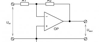
1. Inverting amplifier:
2. Non-inverting amplifier:
Repeater (buffer):
Op-amp AC amplifier:
3. Integrators:
4. Differentiator on op-amp
What determines the power of the circuit?
This scheme has limitations. You can change VT1 KT315 to a more powerful one, which will have a higher gain, but this gain limit is not infinite.
First of all, it all depends on the transistor used. If you change it to a more powerful one, then the gain will be higher. But it should be remembered that the more powerful the transistor, the more powerful the input signal is needed. In addition, you will have to recalculate all components. And connect the preamplifier, assemble the power supply circuit, and this will be a completely different circuit.
Transistors have a number of parameters that affect the circuit. This is the gain for current (h21e), voltage, power. Another important parameter is the power dissipation on the collector. As power increases, a radiator will be required to remove heat.
Amplifier classification
All amplifiers can be classified according to the following criteria:
By frequency of the amplified signal:
- low frequency amplifiers (LF) for amplifying signals from tens of hertz to tens or hundreds of kilohertz;
- broadband amplifiers that amplify signals of units and tens of megahertz;
- selective amplifiers that amplify signals of a narrow frequency band;
By type of signal being amplified
- DC amplifiers (DCA), amplifying electrical signals with a frequency of zero hertz and higher;
- AC amplifiers that amplify electrical signals with a frequency other than zero;
By functional purpose
- voltage amplifiers, current amplifiers and power amplifiers depending on which parameter the amplifier amplifies. The main quantitative parameter of the amplifier is the gain.
Depending on the functional purpose of the amplifier, amplification factors are distinguished by voltage KU, current Ki or power KR:
КU = Uin / Uout
КI= Iin/ Iout
КP= Pin / Pout
where Uin, Iin are the amplitude values of the variable components of voltage and current at the input, respectively;
Uout, Iout are the amplitude values of the alternating components of the voltage and current at the output, respectively;
Rin, Rout - signal powers at the input and output, respectively. Gain factors are often expressed in logarithmic units - decibels:
KU (dB) = 20LgKu
KI(dB) = 20LgKi
KR (dB) = 10LgKp
An amplifier may consist of one or more stages. For multistage amplifiers, its gain is equal to the product of the gains of its individual stages: K = K1 K2 ... Kn
If the gains of the stages are expressed in decibels, then the total gain is equal to the sum of the gains of the individual stages:
K (dB) = K1 (dB) + K2 (dB) +... + Kn (dB).
Typically, the amplifier contains reactive elements, including “parasitic” ones, and the amplification elements used have inertia. Because of this, the gain is a complex quantity:
ЌU = КU ejφ
КU = Uout / Uin
where KU is the gain module; φ is the phase shift between the input and output voltages with amplitudes Uin and Uout.
In addition to the gain, an important quantitative indicator is the efficiency:
η = Pout / Pist
where Rist is the power consumed by the amplifier from the power source.
The role of this indicator especially increases for powerful, as a rule, output stages of the amplifier.
Quantitative indicators of the amplifier also include the input Rin and output Rout resistance of the amplifier:
Rin = Uin / Iin
Rout = |∆ Uout | / |∆ Iout |
where Uin and Iin are the amplitude values of voltage and current at the amplifier input;
∆Uout and ∆Iout are increments in the amplitude values of voltage and current at the amplifier output caused by changes in load resistance. Let us now consider the main characteristics of amplifiers.
Watch an interesting video about the amplifier parameters below:
How to assemble a circuit
The circuit can be assembled on a PCB or on a breadboard. Follow the link to this article, it describes in more detail the process of assembling and testing the circuit.
Use quality parts and good solder. She's working. This is generally a classic circuit for connecting a bipolar transistor with a common emitter.
Also on the site there are other amplifier circuits that are not difficult to assemble and not expensive in terms of the cost of parts.