Electronics is one of the advanced fields of science and technology, which deals with the development and practical application of various electronic devices and devices. From the first years of his life, a child is already faced with a mass of electronic devices. People of all ages are showing a desire to learn the basics of modern electronics for beginners. This article provides the concepts on which the basics of electronics are based.
The simplest tutorial
Ways of improvement (microminiaturization)
Since the advent of solid-state electronics, it has begun to develop at a pace of mathematical progression. Active radioelements, compared to old prototypes, have decreased in size by thousands of times. Some details began to be measured in nanometers. Large electrical circuits began to fit into one chip (microcircuit).
The introduction of new technologies paved the way for the dramatic development of microelectronics. This can be seen from the improvement of cellular communication devices. In a relatively short period of time, a simple cell phone has turned into a smartphone with enormous capabilities. Bulky, low-power computers have been replaced by laptops. Many different miniature electronic gadgets have appeared. Progress in improving electronics industry products is only gaining momentum every day.
Educational electronics for beginners should begin with mastering textbooks and video programs on the basics of digital electronics. You need to understand what microcircuitry and practical electronics are, how circuits are made in electronic circuits. Tutorials will step by step enable the student to learn the basics of electronics.
Electronic circuit board
Chip series
Analog and digital microcircuits are produced in series. A series is a group of microcircuits that have a single design and technological design and are intended for joint use. Microcircuits of the same series, as a rule, have the same power supply voltages and are matched in terms of input and output resistances and signal levels.
Housings
Surface Mount IC Packages
Main article: Types of IC Packages
Microassembly with an open-frame microcircuit welded onto a printed circuit board
The microcircuit housing is a structure designed to protect the microcircuit crystal from external influences, as well as for ease of installation of the microcircuit into an electronic circuit. It contains the housing itself made of dielectric material (plastic, less often ceramic), a set of conductors for electrically connecting the crystal with external circuits through leads, and markings.
There are many options for microcircuit packages, differing in the number of microcircuit pins, installation method, and operating conditions. To simplify installation technology, chip manufacturers are trying to unify packages by developing international standards.
Sometimes microcircuits are produced in an unpackaged design - that is, a crystal without protection. Packless microcircuits are usually designed for installation in a hybrid microassembly. For mass-produced cheap products, direct mounting on a printed circuit board is possible.
Specific names
Intel company
was the first to produce a microcircuit that performed the functions of a microprocessor (English microprocessor) -
Intel
4004. Based on the improved microprocessors 8088 and 8086, IBM
released
its famous personal computers.
The microprocessor forms the core of the computer; additional functions, such as communication with peripherals, were performed using specially designed chipsets (chipset). For the first computers, the number of microcircuits in sets was in the tens and hundreds; in modern systems it is a set of one, two or three microcircuits. Recently, there have been trends in the gradual transfer of chipset functions (memory controller, PCI Express
) to the processor.
Microprocessors with built-in RAM and ROM, memory and I/O controllers, and other additional functions are called microcontrollers.
Microcircuitry
Radio engineering for beginners
It is a branch of microelectronics that deals with the research and development of electrical structural designs of circuits in integrated circuits. They are microelectronic products that perform the functions of conversion, signal processing and information storage.
Important! Microcircuits have a high density of connected elements over an area of several mm2. Their elements cannot be separated from the crystal and substrate.
Microcircuitry
Circuit engineers are engaged in the design and installation of integrated circuits (ICs). There are several types of MI:
- film - all elements and inter-element components are made in the form of films;
- hybrid – contain crystals;
- analog – designed for processing signals that vary according to the law of a continuous function;
- digital – signal processing according to the discrete function law.
First chip 
I am very pleased to talk in detail about my first integrated circuit and share the ups and downs of this project, which I have been working on over the past year. I hope my success will inspire others and help start a revolution in home chip manufacturing. When I started this project, I had no idea what I was getting myself into, but I ended up learning more than I ever thought about physics, chemistry, optics, electronics, and many other fields. In addition, my efforts have been met with only the most positive feedback and support from all over the world. I am sincerely grateful to everyone who helped me, gave me advice and inspired me on this project. Especially my amazing parents, who not only always support and encourage me as much as they can, but also provided me with a workspace and put up with the energy costs... Thank you!
Without further ado, I present the first integrated circuit (IC) manufactured by lithography in the home (garage) - the Z1 dual differential amplifier PMOS chip. I say lithographically manufactured because Geri Ellsworth made the first transistors and logic gates (with connections carefully hand-laid with conductive epoxy) and showed the world that it was possible. Inspired by her work, I present integrated circuits created by a scalable, standard photolithographic process. Needless to say, this is a logical step forward from my previous work where I reproduced Jeri's FET.
I developed the Z1 amplifier when I was looking for a simple chip to test and tune my process. The prototype is made in Magic VLSI for the PMOS process with four masks (active/doped region, gate oxide, contact window and top metal layer). PMOS has an advantage over NMOS when you factor in ionic impurities due to garage manufacturing. The masks are designed with a 16:9 aspect ratio for easier projection.
Magic VLSI Layout
Mask generation
Active area
Gate
Contact
Metal
The gate size is approximately 175 µm, although the chip has features as small as 2 µm for testing. Each amplifier section (center and right) contains three transistors (two for a differential pair with a common resistor in the emitters and one as a current source/load resistor), which means a total of six transistors per IC. On the left side are resistors, capacitors, diodes and other test elements to study the characteristics of the process. Each differential pair assembly comes out with a separate pin on the lead frame so it can be studied and external offset added if necessary.
The manufacturing process consists of 66 separate steps and takes approximately 12 hours. The yield reaches 80% for large elements, but is highly dependent on the amount of coffee consumed on a particular day. I also recorded a video on YouTube about the theory of chip manufacturing and separately about the manufacture of MOSFETs.
50 mm (2″) silicon wafers are cut into 5.08 x 3.175 mm crystals (approx. 16 mm² area) by an Epilog fiber laser. This die size was chosen to fit into Kyocera's 24-pin DIP package.
N-type plate 50mm
N-type plate 50mm
First, the native oxide is removed from the plate by rapid immersion in dilute hydrogen fluoride, followed by intensive treatment with a piranha etching mixture (a mixture of sulfuric acid and hydrogen peroxide), a mixture of RCA 1 (water, ammonia, hydrogen peroxide), a mixture of RCA 2 (water, hydrochloric acid, hydrogen peroxide) and repeated immersion in hydrogen fluoride.
The protective oxide is thermally grown in ambient water vapor (wet oxidation) to a thickness of 5000−8000 Å.
Wet thermal oxidation
Wet thermal oxidation
Tube furnace
Oxidized plate
The oxidized wafer is ready to be patterned on the active/doped (P-type) region. Photoresist AZ4210 is applied to a substrate rotating at approximately 3000 rpm, forming a film about 3.5 microns thick, which is carefully dried at 90°C on an electric stove.
Lithography process in detail
The core mask is processed by my Mark IV photolithographic stepper in ultraviolet with a step of 365 nm - and the structure is processed in a solution of potassium hydroxide.
Resist structure
Resist structure
30 minute drying
Core etching
The resist structure is then tightly solidified and a few other tricks are applied to ensure good adhesion and chemical resistance during the next hydrogen fluoride etch, which transfers that structure to the gate oxide layer and opens windows to the bare silicon for doping. These regions will later become the source and drain of the transistor.
Particles close the gate
Doped crystals with etched gates
After this, doping is carried out, that is, the introduction of impurities from a solid or liquid source. A boron nitride disk placed close (less than 2 mm) to the plate in a tube furnace is used as a solid source. Alternatively, a liquid source can be prepared from phosphoric or boric acid in water or a solvent - and doped using a standard pre-coating/hydrogen fluoride immersion/diffusing/deglazing process.
The above patterning steps are then repeated twice for the gate oxide and contact layer. The gate oxide must be much thinner (less than ~750 Å) than the guard oxide, so the zones between the drain/source are etched away and a thinner oxide is grown there. Then, since the entire wafer has been oxidized during the doping step, the contact windows must be etched to establish contact between the metal layer and the doped source/drain regions.
Now all the transistors are formed and ready for interconnection to the lead frame. A protective layer of aluminum (400−500 nm) is sprayed or thermally sprayed onto the wafer. An alternative would be the lift-off process, where the photoresist is first formed and then the metal is deposited.
Sprayed metal
Sprayed metal
The metal layer is then patterned using photolithography and etched in hot phosphoric acid to complete the integrated circuit. The final steps before testing are visual inspection and high temperature annealing of the aluminum to form ohmic junctions.
The chip is now ready for packaging and testing.
I don't have a microwelding setup (I accept donations!), so testing is currently limited to probing the plate with sharp tweezers or using a flip-chip board (difficult to align) connected to a curve tracer. The differential amplifier is also empirically tested in the circuit to verify functionality.
Curve IV
Curve IV
Of course, these curves are far from ideal (including due to excessive contact resistance and other similar factors), but I expect improved performance if I get my hands on a microwelding setup. This may partly explain some of the differences from crystal to crystal. I will be adding new IV curves, transistor and differential amplifier characteristics to this page soon.
Practical Electronics
The practical study of electronics from scratch begins with an understanding of the operating principles of electronic instruments and devices, the functioning of which is based on the interaction of electromagnetic fields and free electrical charges. Descriptions of these processes can be found in all textbooks on radio and microelectronics. Video lessons on the Internet are especially helpful in this regard. The basics of modern electronics in the practical field are comprehended by acquiring knowledge on the following issues:
- Construction of circuits;
- Semiconductors;
- Signals and measurements;
- Power supply circuits;
- Digital electronics.
Construction of circuits
Electrical Engineering for Beginners
The basis for creating various electrical circuits are the rules for constructing circuits. The same principles for constructing electrical connections apply to the structure of microcircuits. A solid knowledge of the most important laws of Ohm and Kirchhoff allows us to understand the logic of creating lines connecting components of electronic circuits.
Note! Without studying the basic laws of physics and electrical engineering, it is impossible to begin to master the basics of electronics from scratch. It is this knowledge that reveals all the secrets of creating electronic circuits. You can stand for hours watching the operation of certain complex devices, but without knowledge of the basics of electronics, you will not be able to understand the mechanisms of their action.
Semiconductors
In the world of microelectronics, semiconductors occupy an important place. In order to understand the principle of their operation, you need to know their physical capabilities. Semiconductors change their resistance depending on heat. As the temperature increases, the resistance decreases; at low temperatures, semiconductors acquire the properties of dielectrics.
Semiconductors on board
Semiconductors include such radio components as:
- diodes;
- transistors;
- thyristors.
Signals and measurements
Signals are carriers of information. They are transmitted by electrons in an electrical circuit. The magnitude of a charged particle serves as a unit of measurement for energy charge. Measurements and studies of signals in electronics are carried out using oscilloscopes. The digital device performs mathematical processing of the results obtained.
The digital oscilloscope is intended for professional electronics engineers and is quite expensive. For beginner amateurs, inexpensive domestically produced models - C1-73 and C1-101 - are suitable.
Power supply circuits
Energy supply to electronic circuits is carried out through special power supplies. Network switching power supplies are called electronic transformers. These are simple power supplies operating from a 220 volt network. You can buy fairly cheap Chinese-made models on the Internet.
Digital electronics
The basics of digital electronics for beginners are based on the concept of binary system (zero and one) and algebraic logic. Tutorials and various textbooks explain what the basic logical elements of electronic circuits are. These include flip-flops, registers, decoders, and microcontrollers.
Digital electronics
Digital signal transmission technology encodes and, after delivery to the desired location, decrypts them. This ensures the purity of information signals, protected from any interference. An example of this is digital television.
Radio communication
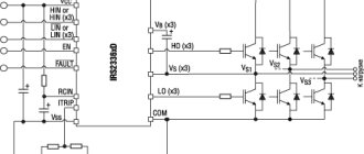
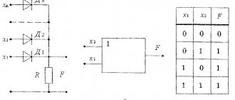
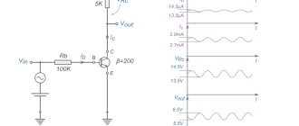
TTL In TTL, the multi-emitter transistor rules the roost. Its essence is that, unlike a conventional bipolar transistor, its emitter structure consists of several (usually 2-3) independent isolated areas adjacent to the base. You can imagine its logical structure by imagining a set of transistors with combined bases and collectors. The resulting sandwich, when turned on in a certain way, performs the functions of AND or OR (sorry for the slight pun). Let's look at the drawing. The input transistor here is precisely this multi-emitter miracle. The logic is simple. While both inputs have high logic levels, the emitter junction is closed and, therefore, at the base of the next transistor, relatively speaking, the level is high. As soon as zero appears at at least one input, the corresponding emitter junction will open and at the base of the next one there will be a voltage close, oddly enough, also to zero. In part, this logic is reminiscent of DTL. The difference is in the use of a transistor, which obviously has better characteristics than individual diodes. The next stage is a complex inverter. This circuit provides lower current consumption than in the case of a single transistor inverter, and also provides, if necessary, a higher output current. Well, the levels will also be closer to zero and nutrition accordingly. Such a scheme can with a clear conscience be called classical, for the reason that while the logical structure remains unchanged, specific solutions can vary significantly. For example, diodes and transistors with a Schottky barrier are now more often used. Its essence is that a thin layer of metal is introduced into the pn junction, which ensures a lower voltage drop across it, and also significantly increases the performance (if anyone is interested, I can say that this is achieved by reducing the lifetime of minority charge carriers in the semiconductor) . There are also TTL MSs with composite transistors at the output; the result is a higher output current (you can already attach a motor to such MS). I also saw a MS with the ability to switch the outputs to the so-called Z-state (or high-impedance, as you like); that is, both output transistors are closed, the output appears as if it is turned off. There were (and are) many variants of TTL, but, as was said, the essence does not change. The advantages of TTL are their diversity. Do you want fast ones, do you want powerful ones, do you want simpler and cheaper ones. There is, perhaps, only one serious drawback. This is the current consumed. He is, let's say, noticeable. No, I don’t argue, it’s quite possible to live, and we lived. And there were again modifications with reduced energy consumption. But this is somehow not the same. Field-effect transistors have conquered many areas from TTL. TTL still makes MCs that are good in every sense, but they will not return the power they once had. Among the domestic series, I can mention K155 and K555 - the most common in amateur radio practice. There are analogues, both complete and modified, both ours and foreign.
Main sections and directions
DIY crafts: DIY electrical
These include:
- studies of processes in vacuum and solid mass;
- study of quantum electronics;
- the path from prototype to finished device.
Vacuum media and solids
The field of vacuum electronics deals with the following:
- design and production of electronic tubes;
- production of microwave magnetrons, klystrons and similar devices;
- production of photocells, indicators and various photoelectronic devices.
Solid state electronics deals with the study and improvement of semiconductors, as well as the manufacture of radio-electronic components based on them. At the same time, this section pays attention to the following issues:
- design and creation of electronic spheres related to crystal growing;
- application of dielectric and metallized films on the surfaces of semiconductors;
- creation of a theoretical basis, supported by practice, for the production of technology for growing films of a given shape and with appropriate technical characteristics;
- search for new solutions to control processes occurring on the surface of semiconductors;
- improvement and development of new technologies for the production of nanoparticles.
Quantum electronics
Quantum electronics studies and creates instruments and devices that process information signals based on the movement of elementary particles. Quantum theory about the properties of electrons and other atomic elements has become the basis for the development of technologies that create powerful lasers. Based on the latest developments in quantum electronics, the prospect of building a quantum computer has emerged.
From prototype to finished product
Due to the exponential improvement of electronic circuits, the path from a prototype of a new electronic device to mass production of a finished product can take from 2.3 to several months. This is noticeable in the constant updating of the range of products on the electronic equipment market.
The acquired knowledge of the basics of electronics will help a beginner in this field to eliminate minor breakdowns, identify and replace damaged components of electronic circuits. This will allow you not to look like a “teapot” in the eyes of electrical engineers who carry out repair work on household electronic devices, which sometimes brings a significant economic effect.