Transistors. Definition and history
A transistor
is an electronic semiconductor device in which the current in a circuit of two electrodes is controlled by a third electrode. (transistors.ru)
Field-effect transistors were the first to be invented (1928), and bipolar transistors appeared in 1947 at Bell Labs. And it was, without exaggeration, a revolution in electronics. Very quickly, transistors replaced vacuum tubes in various electronic devices. In this regard, the reliability of such devices has increased and their size has decreased significantly. And to this day, no matter how “sophisticated” the microcircuit is, it still contains many transistors (as well as diodes, capacitors, resistors, etc.). Only very small ones. By the way, initially “transistors” were resistors whose resistance could be changed using the amount of applied voltage. If we ignore the physics of processes, then a modern transistor can also be represented as a resistance that depends on the signal supplied to it. What is the difference between field-effect and bipolar transistors? The answer lies in their very names. In a bipolar transistor, charge transfer also
electrons
and
holes (“encore” - twice).
And in field (also known as unipolar) there are either
electrons
or
holes.
Also, these types of transistors differ in application areas. Bipolar ones are used mainly in analog technology, and field ones - in digital technology. And finally: the main area of application of any transistors
is amplification of a weak signal due to an additional power source.
Operating principle
Semiconductors occupy an intermediate state between conductors and dielectrics. In their normal state they do not conduct electricity, but their resistance decreases with increasing temperature. The higher it is, the more energy the substance receives.
In semiconductor atoms, electrons break away from the “parent” atom and fly away to another to fill the “hole” left by the same electron. It turns out that two processes occur simultaneously inside such a material: the flight of electrons (n-conductivity, from the word negative), and the formation of “holes” (p-conductivity from the word positive). In an ordinary piece of silicon, these processes are balanced: the number of holes is equal to the number of free electrons.
However, with the help of special substances, this balance can be disrupted by adding “extra” electrons (donor substances) or “extra” “holes” (acceptor substances). In this way, it is possible to obtain a semiconductor crystal with predominant n-conductivity or p-conductivity.
If two such materials are applied to each other, then a so-called pn junction is formed at the point of their contact. Holes and electrons pass through it, saturating its neighbor. That is, where there was an excess of holes, they are filled with electrons and vice versa.
At some point, there will be no free charge carriers left at the point of contact and equilibrium will occur. This is a kind of barrier that cannot be overcome, a kind of desert. This layer is usually called the depletion layer.
Now, if you apply voltage to such a material, it will behave in an interesting way: if it is directed directly, the depleted layer will become thinner and an electric current will flow through it, and if it is directed in the opposite direction, it will expand.
As they say, for dummies, a pn junction has the ability to pass current in only one direction. This is a kind of “check valve” for the electrical network. The operation of all semiconductor devices is based on this property.
There are two main types of transistors: field-effect transistors (sometimes called unipolar) and bipolar. They differ in structure and principle of operation.
Bipolar transistor. Principle of operation. Main characteristics
A bipolar transistor consists of three regions: emitter, base and collector, each of which is supplied with voltage. Depending on the type of conductivity of these areas, npn and pnp transistors are distinguished. Typically the collector area is wider than the emitter area. The base is made of a lightly doped semiconductor (which is why it has high resistance) and is made very thin. Since the emitter-base contact area is significantly smaller than the base-collector contact area, it is impossible to swap the emitter and collector by changing the connection polarity. Thus, the transistor is an asymmetrical device. Before considering the physics of how a transistor operates, let's outline the general problem. It is as follows: a strong current flows between the emitter and the collector ( collector current
), and between the emitter and the base there is a weak control current (
base current
).
The collector current will change depending on the change in base current. Why? Let's consider the pn junctions of the transistor. There are two of them: emitter-base (EB) and base-collector (BC). In the active mode of operation of the transistor, the first of them is connected with forward bias, and the second with reverse bias. What happens at the pn junctions? For greater certainty, we will consider an NPN transistor. For pnp everything is similar, only the word “electrons” needs to be replaced with “holes”. Since the EB junction is open, electrons easily “run across” to the base. There they partially recombine with holes, but most
of them, due to the small thickness of the base and its weak doping, manage to reach the base-collector junction.
Which, as we remember, is reverse biased. And since electrons in the base are minority charge carriers, the electric field of the transition helps them overcome it. Thus, the collector current is only slightly less than the emitter current. Now watch your hands. If you increase the base current, the EB junction will open more strongly, and more electrons will be able to slip between the emitter and collector. And since the collector current is initially greater than the base current, this change will be very, very noticeable. Thus, the weak signal received at the base will be amplified
.
Once again, a large change in collector current is a proportional reflection of a small change in base current. I remember that the principle of operation of a bipolar transistor was explained to my classmate using the example of a water tap. The water in it is the collector current, and the base control current is how much we turn the knob. A small force (control action) is enough to increase the flow of water from the tap. In addition to the processes considered, a number of other phenomena can occur at the pn junctions of the transistor. For example, with a strong increase in voltage at the base-collector junction, avalanche charge multiplication may begin due to impact ionization. And coupled with the tunnel effect, this will give first an electrical breakdown, and then (with increasing current) a thermal breakdown. However, thermal breakdown in a transistor can occur without electrical breakdown (i.e., without increasing the collector voltage to breakdown voltage). One excessive current through the collector will be enough for this. Another phenomenon is due to the fact that when the voltages on the collector and emitter junctions change, their thickness changes. And if the base is too thin, then a closing effect may occur (the so-called “puncture” of the base) - a connection between the collector junction and the emitter junction. In this case, the base region disappears and the transistor stops working normally. The collector current of the transistor in the normal active mode of operation of the transistor is greater than the base current by a certain number of times. This number is called the current gain
and is one of the main parameters of the transistor.
It is designated h21
.
If the transistor is turned on without load on the collector, then at a constant collector-emitter voltage, the ratio of the collector current to the base current will give a static current gain
.
It can be equal to tens or hundreds of units, but it is worth considering the fact that in real circuits this coefficient is smaller due to the fact that when the load is turned on, the collector current naturally decreases. The second important parameter is the input resistance of the transistor
.
According to Ohm's law, it is the ratio of the voltage between the base and emitter to the control current of the base. The larger it is, the lower the base current and the higher the gain. The third parameter of a bipolar transistor is voltage gain
.
It is equal to the ratio of the amplitude or effective values of the output (emitter-collector) and input (base-emitter) alternating voltages. Since the first value is usually very large (units and tens of volts), and the second is very small (tenths of volts), this coefficient can reach tens of thousands of units. It is worth noting that each base control signal has its own voltage gain. Transistors also have a frequency response
, which characterizes the ability of the transistor to amplify a signal whose frequency approaches the cut-off amplification frequency.
The fact is that as the frequency of the input signal increases, the gain decreases. This is due to the fact that the time of occurrence of the main physical processes (the time of movement of carriers from the emitter to the collector, the charge and discharge of capacitive barrier junctions) becomes commensurate with the period of change of the input signal. Those. the transistor simply does not have time to react to changes in the input signal and at some point simply stops amplifying it. The frequency at which this happens is called the cutoff frequency
. Also, the parameters of the bipolar transistor are:
- reverse current collector-emitter
- on time
- reverse collector current
- maximum permissible current
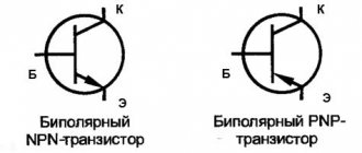
The symbols for npn and pnp transistors differ only in the direction of the arrow indicating the emitter. It shows how current flows in a given transistor.
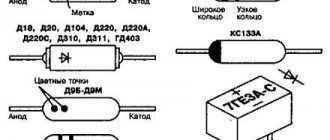
Marking of transistors in accordance with the European classification system.
In accordance with the European classification system, the designation of a transistor consists of two letters and three numbers (devices for general use) or three letters and two numbers (devices for special applications). The first letter characterizes the material from which the transistor is made: A-germanium; B - silicon. The second letter indicates the scope of application of the device: C - low-power low-frequency device; D-powerful low-frequency device; F-low-power high-frequency device; L-powerful high-frequency device. The third letter (if there is one) does not carry any special meaning. For example: transistor AF115 - general purpose, germanium, low-power, high-frequency. Transistor BD135 - general purpose, high power, low frequency.
The figure below shows types of cases of imported transistors.
Field-effect transistor
If in a bipolar transistor the control was carried out using current, then in a field-effect transistor it was controlled using voltage. It consists of a semiconductor plate, which is called a channel. On one side, a source is connected to it - through it, electric current carriers enter the channel, and on the other, a drain - through it they leave the channel.
The channel itself is, as it were, “sandwiched” between a gate, which has reverse conductivity, that is, if the channel has n-conductivity, then the gate has p-conductivity. The gate is electrically separated from the channel. By changing the gate voltage, you can adjust the pn junction area. The larger it is, the less electrical energy passes through the channel. There is a voltage value at which the gate will completely block the channel and the current between the source and drain will stop.
The most obvious illustration in this case is a garden hose that passes through the chamber of a small wheel. In this case, even when a small air pressure is supplied to it (gate-source voltage), it increases significantly in size and begins to pinch the hose, the lumen of the hose is blocked and the water supply stops (the pn junction area increases and electric current stops flowing through the channel).
The type of semiconductor device described above is classic and is called a transistor with a control pn junction. You can often find the abbreviation JFET - Junction FET, which is simply a translation of the Russian name into English.
Another type of field effect triode has a slight difference in gate design. On the silicon layer, a layer of dielectric silicon oxide is formed by oxidation. A shutter is already applied to it by metal spraying. The result is alternating layers of Metal - Dielectric - Semiconductor or MIS gate.
Such an insulated gate field effect transistor is designated by the Latin letters MOSFET.
There are two types of MIS shutter:
- An MIS gate with an induced (or inverse) channel is normally closed, that is, in the absence of voltage on the gate, no electric current passes through the channel. In order to open it, voltage must be applied to the gate.
- An MIS gate with a built-in (or its own) channel is normally open, that is, in the absence of voltage on the gate, electric current passes through the channel. In order to close it, voltage must be applied to the gate.
Checking the functionality of the field-effect transistor
This type of semiconductor elements is also called mosfet and mosfet components. Figure 4 shows the graphic designation of n- and p-channel field switches in circuit diagrams.
Figure 4. Field-effect transistors (N- and P-channel)
To test these devices, we connect the probes to the multimeter in the same way as when testing bipolar semiconductors, and set the test type to “continuity”. Next, we proceed according to the following algorithm (for an n-channel element):
- We touch the black wire to the “c” pin, and the red wire to the “i” pin. The resistance on the built-in diode will be displayed, remember the reading.
- Now you need to “open” the transition (this will only be possible partially), for this we connect the probe with the red wire to terminal “z”.
- We repeat the measurement carried out in step 1, the reading will change downwards, which indicates a partial “opening” of the field worker.
- Now you need to “close” the component, for this purpose we connect the negative probe (black wire) to the “z” leg.
- We repeat steps 1, the original value will be displayed, therefore, “closing” has occurred, which indicates the serviceability of the component.
To test p-channel elements, the sequence of actions remains the same, with the exception of the polarity of the probes, it must be reversed.
Note that insulated gate bipolar elements (IGBT) are tested in the same way as described above. Figure 5 shows the SC12850 component in this class.
Fig 5. IGBT transistor SC12850
For testing, it is necessary to perform the same steps as for a field-effect semiconductor element, taking into account that the drain and source of the latter will correspond to the collector and emitter.
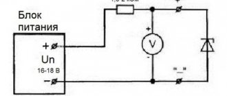
In some cases, the potential on the multimeter probes may not be enough (for example, to “open” a powerful power transistor); in such a situation, additional power will be needed (12 volts will be enough). It must be connected through a resistance of 1500-2000 Ohms.
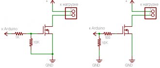
Circuit diagram for connecting field-effect transistors
Three common circuits for connecting field-effect transistors are common. The first circuit is with a common source. The second is with a common drain. The third is with a common shutter. The most common is the common source circuit. It is very similar to a common emitter bipolar transistor circuit. Very large power and current amplification is achieved by a common-source stage.
The common gate circuit is also comparable to one of the bipolar transistor circuits, namely the common base circuit. It does not provide a current amplification, and therefore it is not difficult to assume that the power amplification in it is much less than in a circuit with a common source.
The last scheme - with a common gate - has quite limited use in practice. This is primarily due to the fact that the common gate cascade has an extremely low input resistance.
The difference between bipolar transistors and field effect transistors
Field-effect transistors are controlled using an electric field and due to this they are very energy efficient. It is for this reason that they are used in the production of processors.
On the other hand, field effect transistors have a weak point. This is their thin pn junction. It is very sensitive to static electricity. By the way, it is because of static electricity that flash drives and memory cards stop working if you remove them from the device during operation.
The static electricity protection circuits do not have time to operate, and the static destroys the field-effect transistors.
But bipolar transistors, on the contrary, tolerate static better. But at the same time, they consume more power, since they require electric current to open them.
Marking of transistors in accordance with the Soviet classification system.
For transistors developed before 1964, the type designation consists of two or three elements. The first element of the designation is the letter P, which means that this part is, in fact, a transistor. Bipolar transistors in a sealed housing were designated by two letters - MP, the letter M meant modernization. The second element of the designation is a one, two or three-digit number that determines the serial number of the development and the subclass of the transistor, according to the type of semiconductor material, the values of permissible power dissipation and the cutoff (or limiting) frequency. From 1 to 99 - germanium low-power low-frequency transistors. From 101 to 199 - silicon low-power low-frequency transistors. From 201 to 299 - germanium high-power low-frequency transistors. From 301 to 399 - silicon high-power low-frequency transistors. From 401 to 499 - germanium high-frequency and microwave low-power transistors. From 501 to 599 - silicon high-frequency and microwave low-power transistors. From 601 to 699 - germanium high-frequency and microwave power transistors. From 701 to 799 - silicon high-frequency and microwave power transistors. The third element can be a letter that determines the classification according to the parameters of transistors manufactured using the same technology. For example: MP42 - germanium transistor, low-frequency, low-power, development number - 42 P401 - germanium transistor, low-power, high-frequency, development number - 1.
Starting in 1964, a different designation system was introduced, which was in effect until 1978. Its appearance was associated with the emergence of a large number of new series of various semiconductor devices, in particular field-effect transistors. The following symbols are used to designate the source material (the first element of the designation): Letter G or number 1 - germanium. The letter K or the number 2 is silicon. The letter A or number 3 is gallium arsenide. The second element - the letter T, means a bipolar transistor, the letter P - a field-effect transistor. As the third element of the designation, nine numbers are used that characterize the subclasses of transistors according to the values of power dissipation and cutoff frequency. 1 - low-power (up to 0.3 watt) low-frequency (up to 3 MHz) transistors. 2 - low-power transistors (up to 0.3 watt) of medium frequency (up to 30 MHz). 3 - low-power (up to 0.3 watt) high-frequency transistors. 4-medium power transistors (up to 1.5 watts), low frequency (up to 3 MHz). 5 - medium power transistors (up to 1.5 watts), medium frequency (up to 30 MHz). 6-medium power transistors (up to 1.5 watts), high-frequency and microwave. 7 - powerful transistors (over 1.5 watts), low-frequency (up to 3 MHz). 8- powerful transistors (over 1.5 watts), medium frequency (up to 30 MHz). 9 - powerful transistors (over 1.5 watts), high-frequency and microwave. The fourth and fifth designation elements determine the serial number of the development. Example: KT315A silicon bipolar transistor, low-power, high-frequency, subclass A. Since 1978, changes have been introduced; the first two characters indicating the material and subclass of the transistor have remained the same. The changes affected the designation of functionality - the third element. For bipolar transistors: 1 - transistor with power dissipation up to 1 watt and cutoff frequency up to 30 MHz. 2- transistor with power dissipation up to 1 watt and cutoff frequency up to 300 MHz. 4 - transistor with power dissipation of up to 1 watt and cutoff frequency of more than 300 MHz. 7 - transistor with a power dissipation of more than 1 watt and a cutoff frequency of up to 30 MHz. 8 - transistor with a power dissipation of more than 1 watt and a cutoff frequency of up to 300 MHz. 9 - transistor with a power dissipation of more than 1 watt and a cutoff frequency of over 300 MHz.
The same designations are valid for field effect transistors. To indicate the development serial number, three-digit numbers from 101 to 999 (the next three characters) are used. For additional classification, the letters of the Russian alphabet are used, from A to Z. The number written with a hyphen after the seventh element designates modifications of unpackaged transistors: 1 - with flexible leads without a crystal holder. 2 - with flexible leads on the crystal holder. 3 - with rigid leads without a crystal holder. 4 - with rigid leads on the crystal holder. 5 - with contact pads without a crystal holder and without leads. 6 - with contact pads on the crystal holder, but without leads. Example: KT2115A-2 silicon bipolar transistor for devices of wide application, low-power, high-frequency, unpackaged with flexible leads on the crystal holder. In general, you can’t figure it out without a good catalogue.
Application of transistors in life
Transistors are used in many technical devices. The most striking examples:
- Amplifier circuits.
- Signal generators.
- Electronic keys.
In all communication devices, signal amplification is necessary. First, electrical signals naturally attenuate. Secondly, it often happens that the amplitude of one of the signal parameters is not enough for the device to operate correctly. Information is transmitted using electrical signals. In order for delivery to be guaranteed and the quality of information to be high, we need to strengthen the signals .
Transistors can influence not only the amplitude, but also the shape of an electrical signal. Depending on the required shape of the generated signal, the appropriate type of semiconductor device will be installed in the generator.
Electronic keys are needed to control the current strength in the circuit. These switches contain many transistors. Electronic keys are one of the most important elements of circuits. They are the basis for computers, televisions and other electrical appliances, which are indispensable in modern life.
Transistor color coding
This marking uses colored dots to encode the parameters of transistors in KT-26 (TO-92) and KTP-4 packages. With full color marking, the coding of the nominal value, group and date of issue is applied on a cut of the side surface according to the accepted color scheme.
The dot indicating the standard rating is placed in the upper left corner. It is the starting point. Next, three dots are drawn clockwise, indicating the group, year and month of production, respectively.
When abbreviating the color marking, the release date is omitted (indicated on the package insert). The standard rating is indicated on the cut side surface of the housing. The group is indicated on the end of the body.
Symbolically - color marking of transistors
A distinctive feature of this marking is the absence of numbers and letters. The type rating of the transistor is indicated on the cut side surface with a special symbol (dots, horizontal, vertical or dotted lines) or a colored geometric figure (circle, semicircle, square, triangle, rhombus, etc.). The group marking refers to one (several) points on the end of the body (KT-26, KTP-4).
The color scheme of the dots indicating the group for this marking does not coincide with the standard color scheme according to GOST 24709-81. It is determined by the manufacturer.
The circle symbol on the side cut of the transistor must be distinguished from the point, which does not have a clear shape, because applied with a brush.
Marking of the year and month of manufacture of electronic components
According to GOST 25486-82 , in order to indicate the month and year of manufacture of the transistor and other electronic components, letters and numbers are used: the first value is the year, the second value is the month. As for devices manufactured abroad, a four-digit encoding is used to indicate the date of manufacture, where the first two are the year, the next are the model number.
Each year has its own letter:
Year Code
| 1986 | U |
| 1987 | V |
| 1988 | W |
| 1989 | X |
| 1990 | A |
| 1991 | B |
| 1992 | C |
| 1993 | D |
| 1994 | E |
| 1995 | F |
| 1996 | H |
| 1997 | I |
| 1998 | K |
| 1999 | L |
| 2000 | M |
| 2001 | N |
| 2002 | P |
| 2003 | R |
| 2004 | S |
| 2005 | T |
| 2006 | U |
| 2007 | V |
| 2008 | W |
| 2009 | X |
| 2010 | A |
| 2011 | B |
| 2012 | C |
| 2013 | D |
| 2014 | E |
| 2015 | F |
Month marking
Month Code
| January | 1 |
| February | 2 |
| March | 3 |
| April | 4 |
| May | 5 |
| June | 6 |
| July | 7 |
| August | 8 |
| September | 9 |
| October | O |
| November | N |
| December | D |
To indicate the month of issue, not only numbers, but also some letters are used: the months from January to September fully correspond to the numbers, the following ones correspond to the first letters of the name of the month.
Marking of year and month of manufacture
In accordance with GOST 25486-82, two letters or a letter and a number are used to indicate the date. The first character corresponds to the year, and the second to the month. This type of coding is used not only for transistors, but also for other domestic semiconductor elements. On foreign instruments, the date is indicated by four digits, the first two of which correspond to the year, and the last - the week number. Let's consider what the code marking of transistors means, corresponding to the date of manufacture. Year of issue/symbol: 1986 – U, 1987 – V, 1988 – W, 1989 – X, 1990 – A, 1991 – B, 1992 – C, 1993 – D, 1994 – E, 1995 – F, 1996 – H, 1997 – I, 1998 – K, 1999 – L, 2000 – M, etc. Month of issue: the first nine months correspond to the numbers from 1 to 9 (January – 1, February – 2), and the last ones correspond to the initial letters of the word: October – Oh, November - N, December - D.
PRO-ELECTRON (system developed in Europe)
The marking of devices from European manufacturers is somewhat different. The code with which the foreign transistor is marked is a combination of the symbol:
- The symbol number one indicates the material from which the device is made: A – germanium, B – silicon, C – gallium arsenide, R – cadmium sulfide;
- The second symbol indicates the type of transistor: C – low-power device with low frequency; D – powerful element with low frequency; F – low power device with a high frequency level; G – two or more elements are present in one case at the same time; L – device with high power and frequency; S – low-power device with switching function; U – high power switch transistor;
- The third character indicates the product series number: general use products are marked with numbers from 100 to 999; in the case when a letter is written before the digital value, this indicates that this part is manufactured for use in industry or specialized use.
Moreover, the general encoding is sometimes supplemented with a modification symbol. Only the manufacturer himself can determine it.
European PRO-ELECTRON system
Transistors and other semiconductor devices are marked by European manufacturers as follows.
The code is a symbolic notation. The first letter means the semiconductor material: silicon, germanium, etc. The most common is silicon, it corresponds to the letter B. The next symbol is the type of device. Next is the product series number. This number has several ranges. For example, if numbers from 100 to 999 are indicated, then these elements refer to general-purpose products, and if they are preceded by a letter (Z10 - A99), then these semiconductors are considered parts for special or industrial purposes. In addition, an additional device modification symbol may be added to the general coding. It is determined directly by the manufacturer of semiconductor elements. First symbol (material): A – germanium, B – silicon, C – gallium arsenide, R – cadmium sulfide. The second element means the type of transistor: C – low-power low-frequency; D – powerful low-frequency; F – low-power high-frequency; G – several devices in one housing; L – powerful high-frequency; S – low-power switching; U – powerful switching.
Japanese JIS system
Labeling standards developed in Japan are represented by letters and numbers in the amount of 5 pieces:
- The number 1 is the type of semiconductor transistor: 0 is the designation of a photodiode or phototransistor; 1 – diode designation; 2 – designation of the transistor;
- The letter symbol S is affixed to each item issued;
- The third marking element indicates the type of part: A – PNP with high frequency; B – PNP with low frequency; C—NPN with a high frequency level; D - NPN with low frequency level; N – single-junction; J - field-effect transistor with N-channel; K - field-effect transistor with P-channel;
- The number 4 is the series number in the range from 10 to 9999;
- The fifth symbol of the marking indicates a modification. Sometimes this symbol is missing.
There are situations when the encoding contains a 6th character - this is an additional letter N, M or S, which is responsible for the device’s compliance with certain standards. Labeling developed in Japan does not include color coding.
Sources
- https://habr.com/ru/post/133136/
- https://remont220.ru/osnovy-elektrotehniki/1098-tranzistor/
- https://remont220.ru/stati/595-shemy-vklyucheniya-tranzistorov/
- https://go-radio.ru/transistor.html
- https://tyt-sxemi.ru/tranzistor/
- https://tokar.guru/hochu-vse-znat/tranzistor-vidy-primenenie-i-principy-raboty.html
- https://raschet.info/cvetovaja-i-simvolno-cvetovaja-markirovka-tranzistorov/
- https://www.radiodetector.ru/markirovka-tranzistorov/