KOMPAS-3D is a favorite tool of hundreds of thousands of design engineers and designers in Russia and many other countries. It gained national recognition thanks to its powerful functionality, ease of learning and operation, support for Russian standards, and a wide range of industry applications. In this article we will learn how to draw electrical circuits in this program. First of all, you need to download the program itself and its libraries. At the moment, there are quite a few versions of the program, I do it the old fashioned way, I use version 10, the 13th version came out a long time ago. You can download the libraries yourself, whichever ones you want, but at the end of the article in the archive is attached the version of the library with which we will work, this folder is called ESKW.
Part 1. Launching and configuring the program.
After we have installed the program, let's launch it, a welcome window will appear, and then the following window, where we will need to select the type of document in which we will work:
We select create “Drawing”, a default document in A4 format will open.
If the diagram that you will draw is three-dimensional, then it is better to change the sheet format, say to A3 and place the sheet horizontally. To do this, go to the SERVICE -> DOCUMENT MANAGER menu, change the settings, then save and close the window.
For comfortable work, I advise you to make the following settings: go to the SERVICE menu -> SETTINGS -> CURRENT WINDOW -> SCROLL RAR. Place a check mark on the horizontal and vertical rulers:
Next, download the ESKW library, download the archive at the end of the article, unpack it, and copy it to the root of the folder where the KOMPAS program is installed. Then click SERVICE -> LIBRARY MANAGER, columns will appear at the bottom of the program, right-click on one of the folders and select ADD DESCRIPTION -> APPLICATION LIBRARY.
In the window that appears, find the ESKW folder, which you unpacked and copied to the root of the program folder, go to this folder and select the file called “eskw”, click OPEN.
A new library will appear in the list of libraries at the bottom of the program, put a checkmark on it and open this library; when you launch the library, a message will appear; without reading it, click OK.
This window will appear, where we will select the radio components we need: resistors, capacitors, diodes, etc. We don’t close this window, you can just collapse it.
At this point, setting up and preparing the program for work is completed, now you can start drawing the diagram.
Part 2. Drawing a diagram.
So, the program window ready for use should look like this:
Let's draw a diagram of a simple power supply, start with a transformer, select the element we need in the library, namely a transformer (magnetoelectric), then click the symbol that appears on the sheet to secure it. You can scale (increase or decrease the size) the sheet with the mouse wheel, or cancel the action using the ESC button on the keyboard. To remove a pinned element from a sheet, simply click on it and press the Delete button on the keyboard.
Next, we need to draw a diode bridge and connect it to a transformer, close the library window with transformers, because We will no longer need it, and click on the diode symbol in the library, select the diode bridge in the list of diodes. By the way, when we select an element, another window appears above the element (Rendering Options), where you can rotate, mirror, etc. the selected element.
After we have secured the diode bridge, we need to connect it to the transformer, to do this, on the left side of the program, click on the GEOMETRY symbol (a circle with a triangle), located at the very top, and below select the SECTION symbol. Connecting from point to point, you should get something like this:
Afterwards, in the window with the library, select the electrolytic polar capacitor, rotate it as necessary and fix it on the sheet. Then we connect these elements with lines; to do this, press the CUT button again. To more accurately connect two lines to each other, it is better to increase the scale; by the way, a line attached to a sheet can be lengthened and shortened, just like, for example, in the Sprint Layout program.
Most elements from the output library are short and need to be lengthened using the CUT button. Elements from the library can be destroyed and combined into a macro element, that is, grouped. After you have fixed the capacitor and connected all the elements together with lines, you can draw connectors, and to the transformer, in series with one of the primary windings, you can draw a fuse, and then a connecting plug.
As for connecting lines, the line type can be selected at the bottom of the program, naturally with the CUT button pressed.
Select the dotted line and draw the plug after the transformer.
After you have drawn the diagram, you can proceed to the connection nodes, these are round points at the junctions of the elements. In the library, click on the element CASE - GROUNDING. CONNECTIONS -> CONNECTION UNIT.
And we begin to place the dots; we need to place the dots in this diagram only on the terminals of the capacitor.
Well, that's all, our diagram is almost ready, only something is missing, that's right - inscriptions! To write words and symbols on the diagram, we find the button on the left in the column SYMBOLS, it is usually the third from the top and click on it, a little lower in the same column the buttons will be updated, we find there a button with a picture T, after clicking on the T button, click on sheet, and write the text. After pinning, all symbols, including text, can be easily dragged to any location.
The font, as you probably already understood, changes at the bottom of the program when the T button (text input) is pressed.
The diagram is ready, now you can print it!
Generally speaking, the program is not complicated, intuitive and easy to learn. If you have ever worked with, say, the Sprint Layout program, then you will understand this program very quickly.
As for saving documents, I recommend saving using the “SAVE AS” button and selecting the compass program version 9 from the list, because problems may arise with other formats, and if you save the file as a picture, you will lose the ability to edit the file, and you will have to draw the diagram again.
Before exiting the program, you need to close the library, otherwise the program will complain:
When I was learning the program, I didn’t understand why this error was coming out, it turned out that I minimized the window with the library and didn’t notice it.
2.2 Electrical circuit design
When creating a new drawing, you must go to the File
—
Create
and in the “New Document” window that appears, shown in Figure 1, select the
Drawing
Figure 2 – View of the “New Document” window
A window with an A4 sheet and frame, shown in Figure 2, will appear in the work area.
Figure 3 – View of a window with a sheet and a frame, A4 format
If the diagram that you will draw is three-dimensional, then it is better to change the sheet format, say to A3 and place the sheet horizontally. To do this, go to the SERVICE -> DOCUMENT MANAGER menu, change the settings, then save and close the window.
Figure 4 - Selecting a sheet format
After clicking the Ok button, the sheet format and position will change.
Open the Compass 3D program, find in the tab
Library -> Library for designing ES circuits -> Catalog -> Elements of electrical devices, then select the element we need and insert it into the sheet. We repeat a similar action for all elements.
Capacitor
— a two-terminal network with a certain capacitance value and low ohmic conductivity; a device for accumulating charge and energy of an electric field. A capacitor is a passive electronic component. Usually consists of two electrodes in the form of plates (called plates), separated by a dielectric, the thickness of which is small compared to the size of the plates.
Figure 5 – Capacitor
Electric throttle
- an inductor with high resistance to alternating current and low resistance to direct current. Usually included in a direct current electrical circuit to suppress or limit the alternating component and current ripple. Chokes usually have a core (electrical steel or ferrite). They are mainly used in filters for power supply units.
Figure 6 – Electric throttle
Disconnector
- this is a device designed to create a visible gap between parts of an electrical installation that remain energized and devices taken out for repair, as well as grounding disconnected areas using grounding knives.
A disconnector is capable of opening and closing a circuit with a small current or small change in voltage at the terminals of each of its poles. It is also capable of carrying currents under normal circuit conditions and carrying currents for a normal time under abnormal conditions such as a short circuit.
Small currents are currents such as capacitive currents of bushings, busbars, connections, very short cables, currents of permanently connected step resistances of switches and currents of voltage transformers and dividers. For rated voltages up to and including 330 kV, a current not exceeding 0.5 A is considered a low current by this definition; for rated voltages from 500 kV and above and currents exceeding 0.5 A, it is necessary to consult the manufacturer, unless there are special instructions in the operating instructions for the disconnectors.
Small voltage changes include voltage changes that occur when inductive voltage regulators or switches are bypassed.
For disconnectors with a rated voltage of 110 kV and above, equalizing current switching can be installed.
Figure 7 - Disconnector
Current transformer (meter)
has high accuracy, excellent thermal stability and a standard two-wire 4-20 mA analog output with screw terminal connection.
A wire with the measured current is passed (preferably perpendicular) through the hole of a non-contact transformer. To increase sensitivity, it is allowed to pass the wire several times (turns), and the sensitivity increases as many times as the number of times the wire passes through the hole - for example, a full turn doubles the sensitivity.
Figure 8 – Current meter transformer (in general form)
Switch
is an electrical device designed to limit the current in electrical circuits. The switch protects devices connected in series to it from damage by electric current, while the device is any electrical product through which, in series with the automatic switch, electric current flows. Protected electrical products include both household appliances and other protection devices, as well as the wires and cables themselves, which are called electrical wiring at the household level. Basically, switches serve to protect electrical circuits from overloads and short circuits.
Figure 9 – Switch
Figure 10 - Repetition of circuit elements
Arrester
- an electrical device designed to limit overvoltages in electrical installations and electrical networks. Initially, a surge protection device based on spark gap technology was called a surge arrester. Then, with the development of technology, devices based on semiconductors and metal-oxide varistors began to be used to limit overvoltages, in relation to which the term “arrester” continues to be used.
schemapedia
KOMPAS-3D is a favorite tool of hundreds of thousands of design engineers and designers in Russia and many other countries. It gained national recognition thanks to its powerful functionality, ease of learning and operation, support for Russian standards, and a wide range of industry applications. In this article we will learn how to draw electrical circuits in this program. First of all, you need to download the program itself and its libraries. At the moment, there are quite a few versions of the program, I do it the old fashioned way, I use version 10, the 13th version came out a long time ago. You can download the libraries yourself, whichever ones you want, but at the end of the article in the archive is attached the version of the library with which we will work, this folder is called ESKW.
Part 1. Launching and configuring the program.
After we have installed the program, let's launch it, a welcome window will appear, and then the following window, where we will need to select the type of document in which we will work:
We select create “Drawing”, a default document in A4 format will open.
If the diagram that you will draw is three-dimensional, then it is better to change the sheet format, say to A3 and place the sheet horizontally. To do this, go to the SERVICE -> DOCUMENT MANAGER menu, change the settings, then save and close the window.
For comfortable work, I advise you to make the following settings: go to the SERVICE menu -> SETTINGS -> CURRENT WINDOW -> SCROLL RAR. Place a check mark on the horizontal and vertical rulers:
Next, download the ESKW library, download the archive at the end of the article, unpack it, and copy it to the root of the folder where the KOMPAS program is installed. Then click SERVICE -> LIBRARY MANAGER, columns will appear at the bottom of the program, right-click on one of the folders and select ADD DESCRIPTION -> APPLICATION LIBRARY.
In the window that appears, find the ESKW folder, which you unpacked and copied to the root of the program folder, go to this folder and select the file called “eskw”, click OPEN.
A new library will appear in the list of libraries at the bottom of the program, put a checkmark on it and open this library; when you launch the library, a message will appear; without reading it, click OK.
This window will appear, where we will select the radio components we need: resistors, capacitors, diodes, etc. We don’t close this window, you can just collapse it.
At this point, setting up and preparing the program for work is completed, now you can start drawing the diagram.
Part 2. Drawing a diagram.
So, the program window ready for use should look like this:
Let's draw a diagram of a simple power supply, start with a transformer, select the element we need in the library, namely a transformer (magnetoelectric), then click the symbol that appears on the sheet to secure it. You can scale (increase or decrease the size) the sheet with the mouse wheel, or cancel the action using the ESC button on the keyboard. To remove a pinned element from a sheet, simply click on it and press the Delete button on the keyboard.
Next, we need to draw a diode bridge and connect it to a transformer, close the library window with transformers, because We will no longer need it, and click on the diode symbol in the library, select the diode bridge in the list of diodes. By the way, when we select an element, another window appears above the element (Rendering Options), where you can rotate, mirror, etc. the selected element.
After we have secured the diode bridge, we need to connect it to the transformer, to do this, on the left side of the program, click on the GEOMETRY symbol (a circle with a triangle), located at the very top, and below select the SECTION symbol. Connecting from point to point, you should get something like this:
Afterwards, in the window with the library, select the electrolytic polar capacitor, rotate it as necessary and fix it on the sheet. Then we connect these elements with lines; to do this, press the CUT button again. To more accurately connect two lines to each other, it is better to increase the scale; by the way, a line attached to a sheet can be lengthened and shortened, just like, for example, in the Sprint Layout program.
Most elements from the output library are short and need to be lengthened using the CUT button. Elements from the library can be destroyed and combined into a macro element, that is, grouped. After you have fixed the capacitor and connected all the elements together with lines, you can draw connectors, and to the transformer, in series with one of the primary windings, you can draw a fuse, and then a connecting plug.
As for connecting lines, the line type can be selected at the bottom of the program, naturally with the CUT button pressed.
Select the dotted line and draw the plug after the transformer.
After you have drawn the diagram, you can proceed to the connection nodes, these are round points at the junctions of the elements. In the library, click on the element CASE - GROUNDING. CONNECTIONS -> CONNECTION UNIT.
And we begin to place the dots; we need to place the dots in this diagram only on the terminals of the capacitor.
Well, that’s all, our diagram is almost ready, only something is missing, that’s right – inscriptions! To write words and symbols on the diagram, we find the button on the left in the column SYMBOLS, it is usually the third from the top and click on it, a little lower in the same column the buttons will be updated, we find there a button with a picture T, after clicking on the T button, click on sheet, and write the text. After pinning, all symbols, including text, can be easily dragged to any location.
The font, as you probably already understood, changes at the bottom of the program when the T button (text input) is pressed.
The diagram is ready, now you can print it!
Generally speaking, the program is not complicated, intuitive and easy to learn. If you have ever worked with, say, the Sprint Layout program, then you will understand this program very quickly.
As for saving documents, I recommend saving using the “SAVE AS” button and selecting the compass program version 9 from the list, because problems may arise with other formats, and if you save the file as a picture, you will lose the ability to edit the file, and you will have to draw the diagram again.
Before exiting the program, you need to close the library, otherwise the program will complain:
When I was learning the program, I didn’t understand why this error was coming out, it turned out that I minimized the window with the library and didn’t notice it.
I would like to give one more piece of advice: if you are drawing a diagram for any article, then it is better to convert it into black and white format; a black and white diagram is perceived better than a color one. You can convert it, for example, in the Paint program, just first save the diagram file in JPG format, and in paint, if you save it, select SAVE AS -> monochrome drawing. But as you know, this program (paint) spoils the quality of drawings, I advise you to work in programs such as Paint.net, Lightroom or Adobe Photoshop. Personally, I edit everything in Photoshop, for example, in it you can create and apply interesting effects to a picture.
Here, for example, is a diagram on which a photocopy effect was applied in Photoshop; you must agree, it looks beautiful and very neat than the color version of the diagram.
To create the same effect, open a diagram in JPG format in Photoshop (namely JPEG!), go to the FILTER -> SKETCH -> PHOTO COPY menu, play with the sliders, click OK and save the document.
Below is a short quick video tutorial on how to use the program.
library and drawing
Author: Advanced
We begin designing in KOMPAS-Electric
Today, an integral part of the KOMPAS complex is a specialized application for computer-aided design of electrical equipment KOMPAS-Electric. It operates under the control of the KOMPAS-3D system and is used in the development of any objects in which wired installation is used to make electrical connections. These include low-voltage complete devices (LVDs), relay protection and automation systems (RPA), automated control systems for technological processes, and much more. The system can be used in design institutes, design bureaus and departments that design electric drives and various non-standard equipment.
In our opinion, the process of designing electrical equipment “from top to bottom,” that is, “from the electrical circuit diagram,” is the most correct. This procedure allows you to automatically receive all “downstream” documents: tables and wiring diagrams, lists of elements, lists of purchased products, specifications and other reports. At the same time, in the KOMPAS-Electric system you can design not only in the above sequence, but also in a free order. True, the degree of automation in this case is significantly reduced.
Arranging standard elements on a panel using array commands
Select standard fasteners from the library
Electrical devices most often consist of standard elements used in a variety of products. Creating and accumulating a database of such elements is one of the top priorities, since the presence of such a database significantly speeds up the design process. Standard tools KOMPAS-Electric and KOMPAS-3D allow you to create your own databases (libraries of components) without the use of programming.
Library elements, which can be used as individual parts or assemblies, can be made parametric. Parameterization, together with the mechanism for working with variables, makes it possible to create groups of similar parts that differ in certain parameters. When creating a library using KOMPAS-3D, it is very useful to immediately, directly in the part (subassembly) file, create the corresponding specification object.
This simple action solves several problems at once - when inserting a component into an assembly, you don’t need to remember whether we included it in the specification or not, as well as how many times this component was used (when inserting other exactly the same products, KOMPAS-3D will simply sum up their number) . Filling out databases in the KOMPAS-Electric application is carried out with the help of special assistants - Save Masters.
The resulting three-dimensional model of the board (and a panel with converter commands)
Placing the printed circuit board in the device
The progress of the project of the electrical technical part of the product is optimized using a special Project Manager. At the same time, the project can include not only documents created directly in KOMPAS-Electric, but also any other KOMPAS-3D documents. After completing the design of all diagrams and tables, as well as the preliminary placement of components on the working surfaces of the future product, you can begin the three-dimensional layout.
Let's continue to study together
At the time of publication of this article, the next version of KOMPAS-Electric is being prepared for release. The main emphasis in this version was on improving the quality of the system, which was carried out by optimizing the algorithms of its kernel.
In the previous article (“CAD and Graphics” No. 5, 2004 “KOMPAS-Electric - learning together. Working with databases”) we looked at the “heart” of the system - the database. Now we will talk about the Scheme and Report Editor , with the help of which electrical equipment project documents are produced. More precisely, about the strategy for working on the project, entering initial data and constructing a circuit diagram.
The diagram and report editor is built on the basis of the KOMPAS-Graphic drawing and graphic system. KOMPAS-Electric expands the provided basic set of tools for constructing geometric objects and developing text documents in the “side” of electrical engineering.
Working in the Scheme and Report Editor begins with creating a project . In KOMPAS-Electric terms, a project is a set of documents for the manufacture and maintenance of electrical equipment of the product being electrified. A project is a single file, which, using the Project Manager built into the Scheme and Report Editor, is expanded into a project tree (Fig. 1).
The product developed by KOMPAS-Electric consists of electrical devices installed on supporting structures - surfaces (panels, walls, consoles). These surfaces, in turn, are installed in shells (drawers, cabinets, chambers), thereby becoming elements of its design. The product structure is represented in the Project Manager as a tree at the Components level.
A designer can start working on a project in different ways: by entering initial data for the project (by selecting components) or by developing project documents. Moreover, this can be any project document. However, we recommend starting with the electrical circuit diagram. The two indicated options for starting work may well overlap - the system does not have a strictly defined technological design sequence, which distinguishes it favorably from a number of competing analogues.
When entering the initial data, the designer determines the number of shells and their types, which can be selected from the database or described manually. “Inside” shells, surfaces are described and, if necessary, they are assigned types from the database or they are entered manually. And already on the surface, devices are added directly from the components database. When a device is added, it is assigned a tag , which is the main identifier in the project. As work on the project progresses, the designer can move devices both between the surfaces of the same shell and between different shells of the product.
Each device in the product can be assigned an accompanying element , which can be structural elements (brackets, racks, etc.) or other electrical devices. In the latter case, it becomes possible to expand the initial set of functional parts of the main device (for example, attaching a contact attachment to a magnetic starter allows you to expand its set of free contacts). Thus, related items are additional order items.
When an electrical connection appears between devices installed on different surfaces, a terminal . The terminal is added to the terminal block (Fig. 2). The presence of a terminal block on the surface is determined in the system settings. In the absence of a terminal block on the surface, external connections are automatically made directly to the terminals of the devices.
After entering the data, the optimal step is to begin developing the circuit diagram (E3), because it is this that gives a complete picture of the composition of the product and the electrical connections in it (Fig. 3). To develop a circuit diagram, the system provides a number of functions, which we will consider below.
Panel layout
Three-dimensional layout of panels is carried out using standard functions for working with KOMPAS-3D assemblies. Previously created standard parts are extracted from the library and, using a mate mechanism, placed on a previously created supporting structure (panel, rack, shield, etc.).
If there are many identical elements and they are located in a certain order, you can use one of the commands for creating arrays - along a grid, along a curve, according to a pattern (the sample can be any of the already created arrays - in this case, an array of holes in the board).
With fasteners, the situation is even simpler - when inserting from a standard fastener library, we just need to specify the hole in which the fastener is placed and the end surface along which the fastener will be aligned. As already noted, the specification is generated automatically at this moment.
Assembly drawing of the board and specification for the board
Schematic electrical diagram and list of circuit elements
Working with printed circuit boards
As indicated in the product composition diagram, it can contain not only individual electrical components, but also built-in devices based on printed circuit boards - for example, various control or parameter monitoring systems, amplifiers, sensors and much more. To develop them, enterprises must also have electronic CAD. In addition, converter programs are needed to transfer data from one design system to another. Moreover, these converters must be both simple enough for the user and “smart” enough to ensure a high level of integration of the systems used. ASCON offers its customers (among them the largest instrument-making companies in Russia and neighboring countries, as well as well-known aerospace enterprises developing electronic equipment) its own module for producing text design documentation and three-dimensional models of printed circuit boards based on data obtained from electronic CAD systems. Currently three systems are supported: OrCAD from Cadence, P-CAD and Protel from Altium.
A three-dimensional model of a printed circuit board is created based on files imported from ECAD systems. COMPASS reads the data and makes a construction. The results of the converter's work are a three-dimensional dimensional assembly model of a printed circuit board and a library of elements used in the assembly.
The resulting board is a regular KOMPAS 3D assembly, and further actions with it are no different from working with a product created directly in the system. Now it also needs to be placed in a three-dimensional model of the product we are designing.
The body outline is drawn around a pre-created assembly layout. Associative dimensions allow the case to change its geometry when the position of internal components changes
The subtraction command allows you to automatically obtain a cutout in the housing in the shape of a switch intersecting it
The initial information for creating text documentation is the BOM (Bill of Materials) report, which is generated by ECAD systems. For more complete integration with a schematic electrical diagram drawing or a printed circuit board assembly drawing, you must first transfer these drawings from ECAD to KOMPAS-3D. For the P-CAD system, this operation is most correctly performed through the PDIF format. As part of the KOMPAS-3D system, the PDIF Support Library is used for these purposes: it is designed as a standard application and is launched from the Library Manager. From OrCAD and Protel systems, graphic information can be transferred via DXF format. After receiving the board drawing and the schematic diagram drawing, you need to launch Text Converter, select the desired BOM file, from which the converter reads the data and generates a specification or list of elements. The result of the converter's work is two text documents, and each of them is linked to its own graphic document: the list of elements is to the electrical circuit diagram, and the specification is to the assembly drawing of the board.
Changing Schematic Object Properties
Any property of any schema object can be changed at any time. All the properties listed below can be changed centrally in the corresponding properties dialog, which is created for each type of object.
Document or document sheet. For them, you can change any value that is entered in the title block of the drawing, as well as the name. This simplifies the process of searching the project tree for the desired document or sheet. You can change the format and design of a sheet at any time.
Shell. For the shell, you can change the name, type (describe it as an original, or a unified, or a standard product), and also enter a comment.
Surface. For a surface, you can change the name, type (describe it as an original, or a unified, or a standard product), and enter a comment. Here you can also give permission to create a terminal strip for external connections, allow or disable external connections with the surfaces of other shells, and edit external connection routes.
Apparatus. For a device, you can change the position designation and device type. You can enter and change labels applied to supporting surfaces near the device. You can also enter and change texts that appear on diagrams. The system allows you to manage the format of cross-references, assign related elements, view and insert into the diagram from the dialog any type of UGO that is specified in the database specifically for this type of device.
Connectors. For connectors, you can enter the marking of a potential node, display or hide it on communication lines, and enter the number of a line in a group if it is connected to a group communication line. You can also assign a functional net to a potential node and specify a bus name.
Terminal block. For the terminal strip, you can enter a positional designation and select a type from the database, change the composition of the terminals, assign a type for an individual terminal if the terminal strip consists of a set of individual terminals, define the parameters for the graphical representation of the terminal strip in diagrams (the terminal strip is inserted into diagrams in the form of a table).
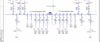
Using the listed functions, the user develops electrical circuit diagrams, one of which is shown in Fig. 6.
The developed schematic diagram is already 70-80% finished project. Most other project documents are obtained automatically. Thus, competent work of specialists in the diagram and report editor can significantly facilitate work and dramatically increase its productivity.
ASCON company presents an updated application to KOMPAS3D V12 for automating the design of power supply systems for residential, public and industrial buildings - the Library for the design of power supply systems: ES. It was created for the development of projects in terms of power electrical equipment (EM), internal electric lighting (EL) and power supply (ES) and is an expanded version of the previously existing Electric Lighting System Design Library: EO.
The new application will help the design engineer to perform routine work much faster and with better quality, which is inevitable when creating and processing project documentation: generating diagrams, counting equipment, creating a cable log, drawing up specifications, marking and much more.
Like many other KOMPAS3D applications for industrial and civil construction, the Power Supply Systems Design Library: ES operates using the MinD (Model in drawing) technology, which combines the advantages of three-dimensional design with the simplicity of two-dimensional design. It integrates components such as KOMPASObject, Construction Site Manager, specialized applications, KOMPASGraphic and KOMPAS3D. The technology invites the designer to start working in the familiar drawing environment (plan view - Fig. 1).
Let's look at how the application works using practical examples.
Rice. 1. Plans for a multi-storey building with electrical supply project
Design of the load-bearing body
It is advisable to design body parts in the context of an assembly, being tied to components previously placed in the assembly. Very often, the housings of many electrical devices are a part bent from a sheet (of steel or aluminum alloys): for its creation, the module for working with sheet material is ideally suited (the new module was described in detail in the magazine "CAD and Graphics" No. 7'2004 ).
Let us recall that the creation of a sheet part begins with the construction of a sheet body based on a sketch, specifying the thickness and coefficient of the neutral layer. To the body created in this way, you can then add other elements of the sheet body (bend, bend along a line, plate, holes, corner closures) or ordinary forming elements (including chamfers, fillets), and the object subtraction command. Let's not forget about the possibility of displaying a sheet part in expanded form. When creating a drawing, you can simultaneously specify both expanded and non-expanded views of the part.
What happened in the end
Window of the Intech-RASKROY W/L system
After development - production
Above we talked about designing the body of our product using the Bending module. Getting a body scan is not an end in itself. One of the serious technological problems solved in production is cutting sheets of metal into blanks for subsequent bending. The task of developing control programs for CNC systems of cutting machines is also very important. Here you can successfully use Intech-RASKROY W/L - a set of programs for automated design of cutting maps, creation of control programs and generation of technological documentation. Thanks to this system, it is possible to increase the utilization rate of sheet metal available in warehouses by up to 95%, since optimal placement of parts and optimal tool paths are ensured, and optimal programs are created for processing on laser, plasma, oxygen and mechanical equipment.
