Suitability of the power supply at home
Everyone in their home has various equipment that runs on batteries or accumulators. In order not to change the elements every time, it is powered from any source connected to a 220 V network.
You should not expect much power from a completely transformerless small-sized unit. Cordless tools (screwdrivers, drills, circular saws), pumps, tablets and laptops will not work on it.
Lighting devices and electronic equipment that consume current up to 500 mA can be connected to such a power supply:
- small-sized receivers;
- LED lamps and garlands (but not ribbons);
- portable low-power medical equipment (wrist blood pressure monitor, pulse meter and other parameters);
- phone charging modules;
- Kids toys;
- tape recorder motors, fans;
- homemade devices;
- Arduino boards.
Transformerless power supplies
In recent years, the interest of radio amateurs in transformerless power supplies (BTBP) has reawakened. With reliable insulation of the powered device (plastic case, absence of external current-carrying parts), such power supplies can be used instead of transformer ones, and in terms of weight and dimensions, a transformerless power supply has noticeable advantages.
In addition to economic feasibility, transformerless power supplies also have other advantages - greater reliability with the correct choice of elements, insensitivity to short circuits at the rectifier output.
A description of the operation of a transformerless power supply and its engineering calculation can be found in [1...3]. In addition to valuable recommendations, V. Bannikov’s article contains a very useful table for radio amateurs for selecting the capacity of a quenching capacitor depending on the given load current.
In addition to the information presented in [1...5], I will add the following from my own experience:
- When choosing a transformerless power supply circuit, absolute preference should be given to a bridge rectifier (Fig. 1). The effective value of the alternating voltage in this circuit, applied to the diode bridge VD1, does not exceed the rectified value - Uo. This allows the use of any small-sized universal diodes with a relatively low maximum permissible reverse voltage - 50...100 V. For example, the widespread D219...D223 with any letter indices, as well as many others.
- As ballast (C1), I use packageless polyethylene terephthalate capacitors of type K73-17 and polypropylene K78-2, used in horizontal scanning circuits of domestic televisions and monitors. Both types of capacitors are specifically designed for operation in alternating, pulsating and pulsed current circuits. The permissible amplitude of the alternating voltage or the alternating component of the pulsating one at a frequency of 50 Hz lies within 55...70% of the rated voltage Un (6). Thus, in transformerless power supply circuits, the specified capacitors with Un = 400, 630 and 1000 V can be used. Another advantage of capacitors with a film (synthetic) dielectric is very low losses and, therefore, negligible heating when operating in alternating current circuits. Thanks to their unframed rectangular design, they occupy a small volume with significant capacity and high operating voltage. Therefore, in contrast to the paper capacitors MBGCh and KGB recommended in [2], film capacitors K73-17, K78-2 easily fit into the housings of small-sized power supplies - adapters.
- I recommend adding fuses to branded and homemade adapters (both transformer and BTBP). If, due to the small volume of the housing, it is impossible to install a fuse holder in the power supply, small-sized inserts PM and VP should be soldered in weight between the pin of the plug and the terminal of the primary winding. The radio industry also produces a modification of VP ceramic fuses with flexible leads for soldering. As a rule, to protect a low-power power supply, a fuse with a current of 0.25 A is sufficient. To eliminate the possibility of short circuits inside the adapter, a small piece of vinyl chloride tube is pulled onto the fuse soldered on one side, and then the other end is soldered.
- At the output of the rectifier of a transformerless power supply, even if it operates on a constant (current) non-switchable load, a zener diode or a transistor voltage stabilizer proposed in [4] should be installed. In this case, if the load circuit is broken, there will be no emergency increase in voltage on the diodes of the rectifier bridge and filter capacitor C2. To increase the reliability of the power supply, I advise you to use non-low-power zener diodes D808...D813, D814A...D. and medium power devices - D815A...Zh, D816A...D, D817A...G. Failure of more powerful zener diodes is much less likely. Since the AC capacitor C1 plays the role of a limiting resistance, an additional ballast resistor to the zener diode VD2 is not required.
- If the power supply is designed to work with a fairly expensive device for which it is dangerous to increase the supply voltage (for example, a pager), an additional protection stage should be installed at the adapter output. This measure is sometimes used in foreign REA to protect IC processors and microcontrollers.
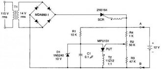
Figure 2 shows a diagram of a simple thyristor device that operates only when there is an emergency increase in voltage at the output of the rectifier or stabilizer. At. this opens a low-power thyristor VS1 through the control circuit, which shunts the rectifier output and causes forced combustion of fuse FU2.
Resistor R2 sets the overload factor. When the ratio of the emergency overload current Iav to the rated current In is from 10 to 20, the melting time of fuses VP1-1 is 2...5 ms. In addition to transformerless rectifiers, quenching capacitors can be used in combined power supplies [5], where the primary winding of the network (isolating) transformer is not designed for the full voltage of the supply network (Fig. 3).
This principle is the basis for the method I have successfully used for remaking low-power power supplies designed for a 120-volt network, or repairing burnt-out ones, for example, when one of the terminals of the primary winding of a 220-volt transformer breaks.
The vast majority of foreign, and many domestic adapters do not have fuses that protect the primary winding of the mains transformer. In the event of an emergency short circuit at the rectifier output (in the load), as well as a breakdown of the rectifier diodes or filter capacitors, instead of a cheap, easily replaceable fuse, the thin wire of the primary winding burns out.
Often, due to technological violations committed during the manufacture of the transformer, over time the wire breaks due to its oxidation at the soldering point of the terminal. If the transformer was designed for two supply voltages - 127/220 V, as a rule, a whole part of the network winding remains for a voltage of 93...127 V.
In this case, as well as when remaking a 120-volt imported adapter, you can restore the power supply for a 220 V network without replacing the transformer. A quenching capacitor is connected in series with the primary winding of the transformer, and by selecting its capacitance, the required distribution of alternating voltages on the capacitor and the primary winding is achieved. The smaller the capacitance of this capacitor, the smaller part of the mains voltage is applied to the transformer winding.
An interesting version of the latter circuit with a symmetrical limitation of the alternating voltage on the primary winding of the transformer was described by L. Pozharinsky in the magazine “Radio”. Zener diodes-limiters VD4. VD5 type D815G are shown with a dotted line in Fig. 3.
All experiments on selecting capacitor capacity and setting up a transformerless power supply must be carried out from a source of regulated alternating voltage (laboratory autotransformer - LATR), starting from zero and up to Uc = 220 V with constant monitoring of the current consumed by the power supply, and in strict compliance with electrical safety rules.
Device and design
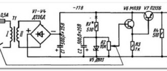
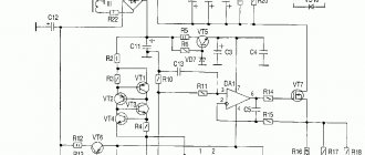
A simple 12-volt power supply without a transformer can be made from several radio elements. It consists of a VD1-4 diode bridge and 3 similar transistor stabilizers connected in series.
Another circuit consists of the following parts:
- 2 capacitors C1 and C2;
- 4 diodes forming a bridge VD1-4;
- 1 zener diode D1.
C1, connected to a 220 V network, extinguishes most of the voltage. It is rectified by the diode bridge VD1-4. Chain D1, C2 is a parametric stabilizer, from the output of which the constant voltage supplying the load is removed.
A more advanced device contains a resistance R1 at the input to suppress the inrush current and an RC circuit - a damping capacitance C1 and a high-value resistor r2 connected in parallel to discharge it. The middle part of the diagram is the same. An additional non-polar capacitor C3 is installed at the output.
Further improvement involves installing a VR1 stabilizer on transistors or a microcircuit at the power supply output.
These blocks are dangerous, since their parts are energized by 220 V. In the absence of load (if the stabilizer is damaged), the output potential will be equal to the network potential.
Electrical circuit diagram
The advantage of this circuit is that excess energy is not dissipated as heat (as with a resistor).
Here, a 200 mA fuse protects the circuit from short circuit or component failure. A 275V varistor protects the circuit from voltage surges. The main part of this power source is capacitor C1 (X type), since the main part of the excess voltage of the mains falls on it.
Resistor R1 is designed to discharge capacitor C1 when the power is turned off, preventing any shock caused by charging the capacitor.
Resistor R2 is designed to prevent excessive transient current that may flow when the power supply is turned on (while C1 is charging). Semiconductors D1...D4 are a bridge rectifier that rectifies alternating voltage. Among them, D1 and D2 are zener diodes, and D3 and D4 are diodes. Thus, the rectified voltage will be limited by the voltage of the zener diodes. Capacitor C2 is a filter capacitor that filters the rectified voltage from noise.
The operation of a transformerless power supply is demonstrated in the above image, which does not require any special explanation.
In the positive half cycle, semiconductors D1 and D4 are forward biased and current flows through the load. The output voltage will be limited by Zener diode D1. In the negative half cycle, semiconductors D2 and D3 are forward biased and the output voltage will be limited by zener diode D2.
Principle of operation
A transformerless transistor unit works as follows. 220 V is rectified by a bridge with a capacitor and supplied to the stabilizers. They are all made according to the same circuit, but are designed for different voltages. The first limits the network potential at 150-180 V, the second stabilizer reduces it by about 2-3 times. The third one produces the required voltage. By changing the zener diode D3, you can get a transformerless power supply, for example, 12 or 5 volts.
The RC block is a voltage divider. In its upper (according to the diagram) arm there is a capacitor C1, which represents a reactive resistance for alternating current (does not consume energy at all). At the bottom there is a diode bridge VD1-4 with a load (zener diode, transistor, microcircuit, etc.).
The input voltage comes to the divider, is rectified by the bridge and goes to the stabilizer, which limits it to the required value.
Transformerless network power supply circuits for microcontrollers
Transformerless power supplies are easier to manufacture and cheaper than transformer ones, but they pose a certain danger to human life during setup, repair and operation. Careless touching of the live part and the grounded surface at the same time can end very disastrously.
Circuits without galvanic isolation are used in those structures where constant human presence is not required or reliable isolation from electric shock is ensured. It is worth noting that it is advisable to use such power supplies only at low load currents, since otherwise the size and cost of the necessary components grow very quickly.
There are the following types of transformerless power supplies:
- with a ballast resistor in the input circuit;
- with a ballast capacitor in the input circuit;
- with a pulse non-isolated AC/DC converter.
Ballast resistors and capacitors suppress excess mains voltage. Accordingly, resistors must be designed for high power dissipation, and capacitors must be film, for example, K73-17, preferably with an operating voltage of at least 630 V. The margin is needed because the permissible AC voltage at a frequency of 50 Hz for this class of capacitors is much less permissible direct voltage KDC (Table 6.2).
Ballast-type circuits “do not like” frequent switching on/off, since voltage surges occur at the initial moment of time. If possible, it is better to do without a network switch altogether, which will significantly extend the life of the device. The optimal scope of application for ballast circuits is low-power devices with round-the-clock operation.
Pulse network transformerless voltage converters are called AC/DC (“variable” AC to “constant” DC). They provide high efficiency and small dimensions, but generate pulsed noise of a fairly high frequency and amplitude. In addition, the microcircuits used in these converters are not cheap and widespread.
In Fig. 6.3, a...m shows transformerless power supply circuits with ballast resistors and capacitors, and in Fig. 6.4, a...g - with microcircuits of pulsed AC/DC converters.
Rice. 6.3. Transformerless power supply circuits with ballast elements (beginning):
a) diodes VD1...VD4 must withstand a reverse voltage of at least 400 V. Resistors Rl, R2 are ballast for the zener diode VD5. The resistance of resistor R3 is selected so that the output voltage does not exceed +5.25 V at any load current. The low-pass filter on elements C1, R3, C2 smooths out network ripples at double frequency 100 Hz;
b) similar to Fig. 6.3, a, but the parallel ballast resistors are replaced by series-connected resistors RL..R3, the RC filter is replaced by the LC filter LI, C1, and the FUI fuse is added. The maximum permissible current through the LI inductor must be greater than the load current by a margin;
c) complete classical circuit of a power supply with ballast capacitor C1. Resistor R1 limits the initial charging current of capacitor C2 and is mandatory in such circuits. Resistor R2 quickly discharges capacitor C1 after disconnecting the plug from the 220 V network. The VD1 diode assembly rectifies the voltage and can be replaced by two diodes of type 1 N4004... 1 N4007. Capacitor C2 smoothes out network ripple, and capacitor C3 eliminates RF interference. The output voltage depends on the parameters of the zener diode VD2 and the load current;
d) power supply from a three-phase network through ballast resistors RL..R3. Zener diode VD4 is needed so that the DA1 microcircuit does not fail from a high input voltage when the load in the +5 V circuit is interrupted or when the current consumption sharply decreases;
Rice. 6.3. Transformerless power supply circuits with ballast elements (continued):
e) Zener diodes VD3, VD4 have increased power dissipation of 1...3 W and perform preliminary voltage limitation. The stabilizer on the DA I chip provides the output voltage;
f) full-wave rectifier with diode bridge VD1 and LED indication of power availability. Resistor R3 determines the current in the load, as well as the brightness of the HLI indicator. The output voltage depends on the parameters of the zener diode VD2 and the load current;
g) bipolar power supply. For complete symmetry of the circuit, it is desirable to provide equal current loads along the +5 and -5 V circuits;
h) dividing the output voltage into two separate branches to eliminate mutual interference, for example, for powering the MK and for controlling the thyristor. Zener diode VD1 limits the voltage at +5.6 V. Diodes VD2, VD3 reduce it to +4.8...+5 V in each channel;
Rice. 6.3. Transformerless power supply circuits with ballast elements (end):
i) receiving two voltages from one power source. The total load current consists of the sum of the currents in the channels +9...+12 V and +5 V. If there are significant fluctuations in the load current, you should choose a VD3 zener diode with increased power dissipation of 1...3 W;
j) Zener diodes VDI, VD2 simultaneously serve as stabilizers and rectifiers. Zener diodes should be chosen that are powerful, with a current reserve;
l) instead of one, two ballast capacitors C1, C2 are used, which can be designed for a lower permissible voltage;
m) in the closed state of thyristor VS1, the current to the transformerless voltage stabilizer (C1...CJ, RL..R3, VDI, VD2) passes through the load RH. Due to the low current value, the load does not operate at full power, for example, the lamp does not light, the fan does not spin, etc. After turning on the VSI thyristor, full power is supplied to the RH load, and the voltage at the stabilizer output decreases from +5 to +2.7 V. For the MK to function normally, it must have a wide-range power supply and be able to organize a restart.
Rice. 6.4. Schemes of network transformerless power supply units with AC/DC converters:
a) a typical circuit for connecting a pulsed AC/DC voltage converter on a DA1 microcircuit from ROHM;
b) a typical circuit for connecting a pulse AC/DC voltage converter on the DA1 microcircuit from Power Integrations. Chokes LI, L2 reduce the level of pulsation;
c) a driver for two popular supply voltages among radio amateurs: +5 and +3.3 V. The DA1 microcircuit is a pulse AC1DC voltage converter from Supertex;
t) DAI is a pulse AC1DC voltage converter from Supertex. The total load current across the +18 and +5 V outputs should not exceed 40 mA.
Source: Ryumik S.M. 1000 and one microcontroller circuit.
Working diagrams
All described devices are made using common radioelements. Below are diagrams indicating all the parts.
In a power supply with transistor stabilizers, the KT940A can be replaced with a high-voltage one that can withstand more than 250 V, and the KT815G with another one with a minimum voltage of 80 V. With the specified details, the device can output up to 300 mA. To increase the current, transistors must be installed on radiators. If you install D814D instead of the KS512A zener diode, the output current of the device will decrease to 200 mA.
A traditional transformerless 12V unit with an RC circuit only produces 20-40mA. If you install a powerful D815Zh zener diode after the bridge, which limits the voltage to 16-19 V, and add a transistor stabilizer to the circuit, the output current will increase to 120 mA. To increase it to 180 mA, it is necessary to solder another similar one in parallel with capacitors C1, C2.
The block on the 78L08 chip (Russian designation KR142B) is more stable. With the specified details, it outputs up to 200 mA.
Calculation of parameters
To prevent breakdown of parts of transformerless circuits, they must be correctly calculated. Each device has its own method.
The transistor unit is calculated according to Ohm's law: U=I×R. It is necessary to calculate the resistances R1, R2, R3 based on the value, voltage and current that each zener diode can withstand.
R=U max/I min.
Calculation of the ballast capacitor for blocks with an RC circuit is carried out using the following formula C = I eff/2*3.14*f *√(Up²-Uв²), where:
- C - ballast capacity (farad);
- Up and Uв — supply and output voltages (volts);
- I eff—load current;
- f is the signal frequency at the device input (hertz).
Since 1 farad = 1 million microfarads, the formula can be simplified:
C = 3200*I eff/√(Uп²-Uв²).
Resistance R1 (kOhm) is approximately equal to 0.025 of the value of the ballast capacitor. Its power should not be lower than 1 W (optimally 2-5 W).
If manual calculation is inconvenient, find and use an online calculator.
General structure and principle of operation
The presented scheme is simple, reliable and efficient. It can be manufactured not only by surface mounting, but also in the form of a printed circuit board. This twelve-volt circuit is working; you only need to calculate in advance the parameters of the ballast quenching capacitor and select the desired current value for a specific device. It is practically possible to make a 5.5-volt unit with the ability to increase the voltage to 25 V.
The basis of the device is a ballast capacitor that suppresses the mains voltage. After this, the current enters the diode rectifier, and the second capacitor acts as a filter. Sometimes it becomes necessary to quickly discharge both capacitors. For this purpose, resistors R1 and R2 are provided in the circuit. Another resistor R3 is used as a current limiter when the load is turned on.
Calculation of the ballast capacitor is performed before assembling the circuit. To do this, use the simple formula C = 3200xI/Uc, in which I is the load current (A), Uc is the mains voltage, C is the capacitance of the capacitor (uF). Most often, such calculations are used for LEDs.
As an example, you can take any device with a current of 150 mA. This could be a regular LED lamp. The mains voltage will be 230 V. Thus, 3200 x 0.15/230 = 2.08 µF. The capacitor value is selected closest to the design value, that is, its capacitance will be 2.2 μF, and the design voltage will be 400 V.