Design and principle of operation of the Li-ion/polymer battery protective controller
Original article here.
If you pick apart any cell phone battery, you will find that a small printed circuit board is soldered to the terminals of the battery cell. This is the so-called protection circuit, or Protection IC . Due to their characteristics, lithium batteries require constant monitoring. Let's take a closer look at how the protection circuit is structured and what elements it consists of.
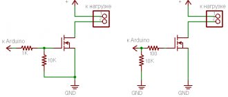
The ordinary circuit of a lithium battery charge controller is a small board on which an electronic circuit of SMD components is mounted. The controller circuit of 1 cell (“bank”) at 3.7V, as a rule, consists of two microcircuits. One control chip, and the other executive - an assembly of two MOSFET transistors.
The photo shows a charge controller board from a 3.7V battery.
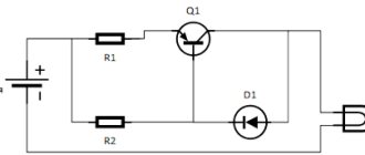
The microcircuit marked DW01-P in a small case is essentially the “brain” of the controller. Here is a typical circuit diagram for connecting this microcircuit. In the diagram, G1 is a lithium-ion or polymer battery cell. FET1, FET2 are MOSFET transistors.
Typical circuit diagram for connecting the DW01-P microcircuit
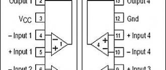
Pinout, appearance and purpose of pins of the DW01-P microcircuit.
MOSFET transistors are not included in the DW01-P microcircuit and are made in the form of a separate microcircuit assembly of 2 N-type MOSFET transistors. Typically an assembly labeled 8205 is used, and the package can be either 6-pin (SOT-23-6) or 8-pin (TSSOP-8). The assembly may be labeled as TXY8205A, SSF8205, S8205A, etc. You can also find assemblies marked 8814 and similar ones.
Here is the pinout and composition of the S8205A chip in the TSSOP-8 package.
Two field-effect transistors are used to separately control the discharge and charge of the battery cell. For convenience, they are manufactured in one case.
The transistor (FET1) that is connected to the OD ( Overdischarge ) pin of the DW01-P microcircuit controls the battery discharge - connects/disconnects the load. And the one (FET2) that is connected to the OC ( Overcharge ) pin connects/disconnects the power source (charger). Thus, by opening or closing the corresponding transistor, you can, for example, turn off the load (consumer) or stop charging the battery cell.
Let's look at the logic of the control chip and the entire protection circuit as a whole.
Overcharge Protection.
As you know, overcharging a lithium battery above 4.2 - 4.3V is fraught with overheating and even explosion.
If the voltage on the cell reaches 4.2 - 4.3V ( Overcharge Protection Voltage - VOCP ), then the control chip closes the FET2 transistor, thereby preventing further charging of the battery. The battery will be disconnected from the power source until the cell voltage drops below 4 - 4.1V ( Overcharge Release Voltage - VOCR ) due to self-discharge. This is only the case if there is no load connected to the battery, for example it is removed from a cell phone.
If the battery is connected to a load, then the FET2 transistor opens again when the voltage across the cell drops below 4.2V.
Overdischarge Protection.
If the voltage on the battery drops below 2.3 - 2.5V ( Overdischarge Protection Voltage - VODP ), then the controller turns off the MOSFET discharge transistor FET1 - it is connected to the DO pin.
Next, the DW01-P control chip will go into sleep mode ( Power Down ) and consume a current of only 0.1 µA. (at supply voltage 2V).
There is a very interesting condition . As long as the voltage on the battery cell does not exceed 2.9 - 3.1V ( Overdischarge Release Voltage - VODR ), the load will be completely turned off. There will be 0V at the controller terminals. Those who are little familiar with the logic of the protective circuit may mistake this state of affairs for the “death” of the battery. Here's just a small example.
Miniature Li-polymer battery 3.7V from an MP3 player. Composition: control controller - G2NK ( S-8261 ), field-effect transistor assembly - KC3J1 .
The battery has discharged below 2.5V. The control circuit disconnected it from the load. The controller output is 0V.
Moreover, if you measure the voltage on the battery cell, then after disconnecting the load it increased slightly and reached a level of 2.7V.
In order for the controller to reconnect the battery to the “outside world”, that is, to the load, the voltage on the battery cell must be 2.9 - 3.1V ( VODR ).
A very reasonable question arises here.
The diagram shows that the Drain terminals of transistors FET1, FET2 are connected together and are not connected anywhere. How does current flow through such a circuit when the overcharge protection is triggered? How can we recharge the battery “can” again so that the controller turns on the discharge transistor - FET1 - again?
The fact is that inside field-effect transistors there are so-called parasitic diodes - they are the result of the technological process of manufacturing MOSFET transistors. It is precisely through such a parasitic (internal) diode of the FET1 transistor that the charge current will flow, since it will be turned on in the forward direction.
If you rummage through the datasheets for Li-ion/polymer protection microcircuits (including DW01-P , G2NK ), you can find out that after deep discharge protection is triggered, a charge detection circuit is in effect - Charger Detection . That is, when the charger is connected, the circuit will detect that the charger is connected and allow the charging process.
Charging to a level of 3.1V after a deep discharge of a lithium cell can take a very long time - several hours.
To restore a lithium-ion/polymer battery, you can use special devices, for example, the Turnigy Accucell 6 universal charger. You can find out how to do this here.
It was with this method that I managed to restore a Li-polymer 3.7V battery from an MP3 player. Charging from 2.7V to 4.2V took 554 minutes and 52 seconds, which is more than 9 hours ! This is how long a “recovery” charge can last.
Among other things, the functionality of lithium battery protection microcircuits includes protection against overcurrent ( Overcurrent Protection ) and short circuit. Overcurrent protection is triggered in the event of a sudden drop in voltage by a certain amount. After this, the microcircuit limits the load current. If there is a short circuit (short circuit) in the load, the controller completely turns it off until the short circuit is eliminated.
Causes of mobile phone charger malfunctions
The most common cause of memory failure is negligence during operation.
Phone charger repair
Possible causes of breakdowns of the mobile phone charging unit
1. Broken wire at the plug and at the base of the charging unit. You can break the wires when charging is on during calls.
You need to pull the plug out of the phone socket not by the wire, but by the plug body.
2. Failure of elements of the electronic board of the charger. Very often the charger is left plugged in and not removed from the outlet. At the same time, the entire electronic board of the charger is constantly under voltage, which reduces the service life of the board's radio elements.
Incorrect order of turning on and off the charger also leads to premature wear of the unit elements.
If you disconnect the phone from the charger under voltage, sudden voltage surges occur that exceed the maximum permissible operating voltages of the elements. This is due to transient processes that occur in the memory when the load is removed (the phone is turned off) under voltage. If the charger is used correctly, the phone is connected and disconnected with the charging switched off.
Insulated gate field effect transistor
MOSFET transistor
Today, among a sufficient number of varieties of transistors, two classes are distinguished: pn - transition transistors (bipolar) and transistors with an insulated semiconductor gate (field-effect). Another name that can be found when describing field-effect transistors is MOS (metal-oxide-semiconductor) due to the fact that silicon oxide (SiO2) is mainly used as a dielectric material. Another fairly common name is MIS (metal-dielectric-semiconductor).
A few clarifications. Very often you can hear the terms MOSFET , mosfet , MOS transistor . This term is sometimes misleading for beginners in electronics.
What is a MOSFET?
MOSFET is an abbreviation for two English phrases: Metal-Oxide-Semiconductor (metal - oxide - semiconductor) and Field-Effect-Transistors (electric field-controlled transistor). Therefore, a MOSFET is nothing more than a regular MOS transistor.
I think it is now clear that the terms mosfet, MOSFET, MOS, MOS, MOS mean the same thing, namely an insulated gate field-effect transistor.
It is worth remembering that along with the abbreviation MOSFET, the abbreviation J-FET (Junction) is used. J-FET transistors are also field-effect transistors, but such a transistor is controlled by using a control pn junction in it. These transistors, unlike MOSFETs, have a slightly different structure.
The operating principle of a field-effect transistor.
The essence of the operation of a field-effect transistor is the ability to control the current flowing through it using an electric field (voltage). This compares favorably with bipolar transistors, where a large output current is controlled using a small input current.
A simplified model of a field-effect transistor with an insulated gate.
Let's take a look at a simplified model of a field-effect transistor with an insulated gate (see figure). Since MOS transistors come with different types of conductivity (n or p), the figure shows a field-effect transistor with an insulated gate and an n-type channel.
Simplified model of a field-effect transistor with an insulated gate
The basis of the MOS transistor is:
- Silicon substrate . The substrate can be either a p-type or an n-type semiconductor. If the substrate is p-type, then the semiconductor contains more positively charged atoms at the sites of the silicon crystal lattice. If the substrate is of type n, then the semiconductor contains more negatively charged atoms and free electrons. In both cases, the formation of a p or n type semiconductor is achieved through the introduction of impurities.
- Semiconductor n+ regions . These regions are highly enriched in free electrons (hence the “+”), which is achieved by introducing an impurity into the semiconductor. The source and drain electrodes are connected to these areas.
- Dielectric . It isolates the gate electrode from the silicon substrate. The dielectric itself is made of silicon oxide (SiO2). A gate electrode, the control electrode, is connected to the surface of the dielectric.
Now let's briefly describe how it all works.
+ is applied between the gate and the source to the gate terminal, then a transverse electric field is formed between the metal terminal of the gate and the substrate. This, in turn, begins to attract negatively charged free electrons, which are dispersed in small quantities in the silicon substrate, to the surface layer of the dielectric.
As a result, a sufficiently large number of electrons accumulate in the near-surface layer and a so-called channel is formed - the conduction region . In the figure, the channel is shown in blue. The fact that the channel is of type n means that it consists of electrons. As we can see, a kind of “bridge” is formed between the source and drain terminals, and, in fact, their n+ regions, which conducts electric current.
Current begins to flow between the source and drain. Thus, due to the external control voltage, the conductivity of the field-effect transistor is controlled. If you remove the control voltage from the gate, the conducting channel in the near-surface layer will disappear and the transistor will close and stop passing current. It should be noted that the simplified model figure shows a field-effect transistor with an n-type channel. There are also field-effect transistors with a p-type channel.
The model shown is highly simplified. In reality, the design of a modern MOS transistor is much more complex. But, despite this, the simplified model clearly and simply shows the idea that was put into the device of a field-effect transistor with an insulated gate.
Among other things, field-effect transistors with an insulated gate are of depleted and enriched types. The figure shows just an enriched field-effect transistor - in it the channel is “enriched” with electrons. In a depletion type transistor, electrons are already present in the channel area, so the transistor passes current without a control voltage at the gate. The current-voltage characteristics of depleted and enriched field-effect transistors differ significantly.
You can read about the difference between enriched and depleted MOSFET transistors here. It also shows how MOS transistors are designated on circuit diagrams.
It is easy to see that the gate electrode and the substrate, together with the dielectric that is located between them, form a kind of electrical capacitor. The plates are the metal gate terminal and the substrate area, and the insulator between these electrodes is a silicon oxide (SiO2) dielectric. Therefore, a field-effect transistor has an essential parameter called gate capacitance .
Field-effect transistors, unlike bipolar transistors, have lower intrinsic noise at low frequencies. Therefore, they are actively used in sound reinforcement technology. For example, modern low-frequency power amplifier microcircuits for car CD/MP3 players contain MOSFET transistors. On the dashboard of a car receiver you can see the inscription “ Power MOSFET ” or similar. This is how the manufacturer brags, making it clear that he cares not only about power, but also about sound quality.
A field-effect transistor, in comparison with bipolar transistors, has a higher input resistance, which can reach 10 to the 9th power of Ohm or more. This feature allows us to consider these devices as potential-controlled or, in other words, voltage-controlled. Today this is the best option for creating circuits with sufficiently low power consumption in static rest mode. This condition is especially relevant for static memory circuits with a large number of storage cells.
If we talk about the key mode of operation of transistors, then in this case bipolar ones show better performance, since the voltage drop across the field options is very significant, which reduces the overall efficiency of the entire circuit. Despite this, as a result of the development of field-effect transistor manufacturing technologies, it was possible to get rid of this problem. Modern field-effect transistors have low channel resistance and work well at high frequencies.
As a result of the search to improve the characteristics of high-power field-effect transistors, a hybrid electronic device was invented - IGBT transistor , which is a hybrid of a field-effect and bipolar transistor.
Adapter for charging your phone in the car
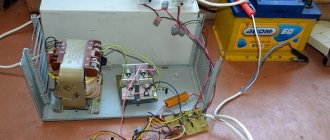
The circuit design of the adapter in question for charging from a car cigarette lighter does not pretend to be original and uses a very common MC34063 microcircuit. However, the PCB is designed to fit the small Z-43 case and takes up little space. This project will be useful for those who would still like to make their own phone charger for a car rather than buy a ready-made device, since the total cost of the devices will probably be the same.
So, let's move on to the device diagram:
The circuit is built on the MC34063 DC/DC converter chip, the chip is used in a DIP-8 package, since the power dissipation in such a package is slightly greater than in an SO-8 package - it’s a little more reliable. Resistors R2 and R3 form feedback to the output of the circuit, as such the resistors form a voltage divider. At the same time, a voltage of 1.25 volts is always maintained at the fifth pin of the microcircuit, which means that the output voltage directly depends on the combination of ratings in the voltage divider:
And from this it follows that the output voltage can be accurately calculated. If we need to get 5 volts at the output, then we need to arbitrarily choose the value of one resistor - let it be 1000 Ohms, then the calculation of the other resistor will look like this:
If the values were not so “beautiful”, then it would be necessary to set a different value at the beginning and recalculate the second resistor.
Resistor R1 is used like a fuse - if the rated current of the microcircuit is exceeded, it will turn it off. Since the value of this resistor is small, it can be assembled from several resistors connected in parallel to each other. This is provided on the printed circuit board. Capacitor C3 sets the operating frequency of the converter. The remaining capacitors perform filtering functions at the input and output. The higher the value of capacitor C5, the less ripple will be at the output. An important parameter for us is miniature size, so the circuit used a 1000 µF capacitor, soldered from the motherboard at 6.3 volts. Diode VD1 must be fast (Schottky). And the inductor must also be selected not only based on its inductance, but on the current that it can pass for a long time without destruction. In this circuit, a choke designed for 1 ampere is quite suitable. The connector at the output of the circuit is USB-A (female). At the input there is a regular connector for power supply of a suitable diameter for you, the type of connector is also female. Thus, the output can be connected to a standard USB cable for your phone or other device. The input of the circuit is connected through the car cigarette lighter adapter. In general, this matter can be simplified a little and connect the cigarette lighter connector simply by soldering the wires to the board, rather than using a connector.
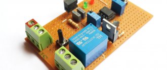
As stated, the body is used by Z-43. The printed circuit board with installed components occupies the entire space of the case. It is necessary to make two holes in the case - for the USB connector and for the input voltage. In the photo, the bottom cover is slightly filed to close tightly due to the dimensions of the cigarette lighter connector. A little grinding in, so to speak. If you refuse to use a connector for the voltage input, the occupied volume in the case will decrease slightly and the hole can be made smaller to feed the wire inside the case in order to be soldered to the contacts on the board. This variation with the connector depends on what is available (I was sorry to cut the cigarette lighter wire, so I used this connector).
On the printed circuit board in Sprint Layout, a jumper is indicated on the blue layer (M1). On the finished printed circuit board this jumper is made with a blue wire.
The finished adapter looks like this:
The size is quite compact.
Adapter in working position:
Adapter Specifications:
- input voltage - 12 V
- output voltage - 5 V
- conversion frequency - 85 kHz
- output current - 500 mA (can be increased to 750 mA by replacing resistor R1 with 0.2 Ohm - this will be the maximum current allowed by the microcircuit)
- Efficiency ~ 70-75%
The article is accompanied by a printed circuit board in the Sprint-Layout 6 program, as well as a proteus project to simulate the operation of the converter circuit.
Attached files:
- DC-DC 12 - 5V housing.lay (23 Kb)
- dc-prot.rar (19 Kb)
Insulated gate bipolar transistor
In modern power electronics, so-called IGBT transistors are widely used. This abbreviation is borrowed from foreign terminology and stands for Insulated Gate Bipolar Transistor, and in Russian it sounds like an Insulated Gate Bipolar Transistor. Therefore, IGBT transistors are also called IGBTs. An IGBT is an electronic power device that is used as a powerful electronic switch installed in switching power supplies, inverters, and electric drive control systems.
An IGBT transistor is a rather clever device, which is a hybrid of a field-effect and bipolar transistor. This combination has led to the fact that this type of transistor has inherited the positive qualities of both a field-effect transistor and a bipolar one.
The essence of the operation of an IGBT transistor is that the field-effect transistor controls a powerful bipolar transistor. As a result, switching a powerful load becomes possible with low control power, since the control signal is supplied to the gate of the field-effect transistor.
The internal structure of the IGBT is a cascade connection of two electronic input switches that control the terminal plus. The following figure shows a simplified equivalent circuit of an insulated gate bipolar transistor.
| Simplified IGBT equivalent circuit |
The entire process of IGBT operation can be represented in two stages: as soon as a positive voltage is applied, a field-effect transistor opens between the gate and source, that is, an n channel is formed between the source and drain. In this case, charges begin to move from region n to region p , which entails the opening of the bipolar transistor, as a result of which current flows from the emitter to the collector.
The history of the appearance of IGBTs.
Power field-effect transistors first appeared in 1973, and already in 1979 a composite transistor circuit was proposed, equipped with a controlled bipolar transistor using an insulated gate field-effect transistor. During the tests, it was found that when using a bipolar transistor as a switch, there is no saturation on the main transistor, and this significantly reduces the delay when the switch is turned off.
Somewhat later, in 1985, a bipolar transistor with an insulated gate was introduced, the distinctive feature of which was a flat structure; the range of operating voltages became larger. Thus, at high voltages and high currents, the on-state losses are very small. In this case, the device has similar switching and conductivity characteristics as a bipolar transistor, and control is carried out by voltage.
The first generation of devices had some disadvantages: switching was slow, and they were not very reliable. The second generation was released in the 90s, and the third generation is still being produced: they eliminate such shortcomings, they have a high input resistance, the controlled power is low, and in the on state the residual voltage is also low.
Already now, IGBT transistors are available in electronic component stores that can switch currents in the range from several tens to hundreds of amperes ( Ike max ), and the operating voltage ( Uke max ) can vary from several hundred to a thousand or more volts.
Symbol of IGBT (IGBT) on circuit diagrams.
Since the IGBT transistor has a combined structure of a field-effect and bipolar transistor, its terminals are called gate - G (control electrode), emitter ( E ) and collector ( K ). , the gate terminal is designated by the letter G , the emitter terminal by E , and the collector terminal by C.
| Symbol IGBT |
The figure shows a conventional graphic symbol for an insulated gate bipolar transistor. The transistor can also be depicted with a built-in fast diode. Also, an IGBT transistor can be depicted as follows:
Schematic diagram
Rice. 1. Voltage stabilizer circuit for +5V.
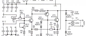
Rice. 2. DC-DC voltage converter circuit based on the MC34063A chip.
The circuit shown in Figure 2 operates as a pulsed source, and during normal operation dissipates very little power.
There is absolutely nothing here that requires heat removal. In addition to the fact that it has a very high efficiency, this scheme allows you to assemble the adapter in the form of a very light and compact structure.
Of course, there is a minus - the circuit is much more complicated, it contains many parts, the total cost of which is significantly more than the price of KR142EN5A and a pair of capacitors.
The “charger” is connected to the car’s cigarette lighter. Just in case, diode VD1 protects the circuit from incorrect polarity of the input voltage (suddenly the cigarette lighter was changed and connected incorrectly). Zener diode VD2 - protection against short high voltage pulses that may be present in the network of a not very new car.
The A1 chip contains the main components of the converter: a pulse generator, a pulse width regulator, and a measuring comparator that compares the output voltage with the reference voltage generated by the internal stabilizer of the chip.
The input of the comparator is pin 5. It is supplied with voltage from the output of the circuit through a divider on resistors R4-R6. The division coefficient depends on the position of the trimmer resistor R5. When setting up the converter, this resistor is used to set the required output voltage (in this case it is 5V).