Good day to all! In the last article, I looked at RC generators of sinusoidal (harmonic) oscillations using an op-amp. In this article I will look at voltage stabilizers, which are based on operational amplifiers. The main advantage of op-amps when used in voltage stabilizers is that the op-amp has a large gain (several tens of thousands). Therefore, they make it possible to obtain an output voltage instability of the order of 0.001%.
To assemble a radio-electronic device, you can pre-make a DIY KIT kit using the link.
Basic circuit of a compensation voltage stabilizer
Most modern power electronics are represented by switching power supplies, which have high efficiency and small overall dimensions. However, linear voltage stabilizers also find their use, primarily in low-power devices, as well as in circuits where impulse noise is not desired.
As is known, linear power supplies are divided into serial and parallel, depending on the connection diagram of the control element relative to the output. Series stabilizers are most widespread, as they can provide efficiency and stabilization greater than parallel ones, the main advantages of which are the possibility of overcurrent and the ability to withstand short circuits.
In addition to the connection diagram of the regulating element, voltage stabilizers are classified according to the method of regulating the output voltage: parametric and compensation. The operation of parametric stabilizers is based on the nonlinear properties of the control elements, that is, with a significant change in the current flowing through it, the voltage drop across the control element changes little. Such stabilizers are used in low-power circuits up to several watts. The most widely used circuits are series stabilizers of the compensation type, the block diagram of which is presented below
Block diagram of a series-type compensating stabilizer.
In one of the articles I talked about compensation voltage stabilizers made on transistors, so let me remind you of the principle of its operation. The circuit consists of four main parts: a reference voltage source I , a comparison element ES , an amplifying element U and a regulating element R. The comparison element compares the output voltage U1 with the voltage generated by the reference voltage source and generates a comparison error to the amplifying element, where the comparison error is amplified and a control signal is generated for the regulatory element.
Quite often, in simple circuits, a comparison element and an amplifier (and sometimes a regulating element in low-current circuits) are combined into one device. In modern circuits, the functions of the comparison element and amplifier are performed on an op-amp.
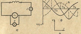
Voltage and current stabilizer circuits
Stabilized power supplies are necessary to ensure that the parameters of an electronic device are independent of changes in the supply voltage. Almost any modern equipment has a voltage stabilizer , or even several. In such devices operational amplifiers ( op-amps ) are often used, with the help of which this problem can be solved simply and effectively with control accuracy and stability in the range of 0.01...0.5%, and the op-amp can be easily integrated into traditional voltage and current stabilizers. The simplest voltage stabilizer is a direct current amplifier, the input of which is supplied with a constant voltage of a zener diode or part of it. The load capacity of such a stabilizer is determined by the maximum output current of the op-amp. Tracking stabilizers , as a rule, work on the principle of comparing the reference and output voltages, amplifying their difference and controlling the electrical conductivity of the control transistor.
The stabilizer according to the diagram in Fig. 1 produces a voltage Uout greater than the reference voltage of the zener diode VD1, and the stabilizer in Fig. 2 produces less. Stabilizers are powered from a single source. Using the emitter follower VT2, the load current is increased, in our example - up to 100 mA, but more is possible with a compound follower on a powerful transistor.
Transistor VT1 protects output transistor VT2 from current overloads, and the current sensor is a small resistance resistor R8 connected to the emitter circuit of transistor VT2. When the voltage drop across it exceeds Ub-e = 0.6 V, transistor VT1 will open and shunt the emitter junction of transistor VT2. For load currents up to 10...15 mA, resistors R7, R8 and transistors VT1, VT2 can be omitted. Note that in zener diodes according to the circuits in Fig. 1, 2, the input voltage should not exceed the maximum permissible sum of supply voltages.
Figure 3a shows a diagram of such a stabilizer in which the op-amp is connected in such a way that it itself is powered by a stabilized voltage. Several elements are additionally included here that improve the operation of the voltage stabilizer. The output potential of op-amp DA1 is shifted towards positive voltage using zener diode VD3 and transistor VT1. The output emitter follower is composite (VT2, VT3), and a divider R4R5 is connected to the base of the protective transistor VT4, which allows you to create a “falling” characteristic of overload current limitation. The short circuit current does not exceed 0.3 A.
The temperature-compensated reference voltage source is made on the K101KT1A (DA2) microcircuit . The output voltage of the stabilizer, equal to +15V, changes by only 0.0002% when the input voltage changes within 19...30 V; when the load current changes from zero to the rated value, the output voltage drops by only 0.001%. In this stabilizer, the ripple suppression of the input voltage with a frequency of 100 Hz is 120 dB. The advantages of the stabilizer also include the fact that in the absence of a load, the current consumption is about 10 mA. When the load current changes abruptly, the output voltage is set with an error of 0.1% in a time of no more than 5 μs.
Almost zero voltage ripple at the output can be provided by a stabilizer according to the circuit in Fig. 4. If the motor of the variable resistor R1 is in the upper (according to the diagram) position, the ripple amplitude is maximum. As the slider moves down, the amplitude will decrease, since the ripple voltage supplied to the inverting input of the op-amp through capacitor C2 is added in antiphase to the output ripple voltage. At approximately the middle position of the resistor R1 slider, the ripples will be compensated. If it is necessary to obtain a negative output voltage, it is necessary to use a pnp transistor as a repeater, and also ground the positive power bus of the op-amp . But you can do it differently if the equipment requires stabilized voltages of different polarities.
Figure 5 shows two simplified diagrams for connecting stabilizers to obtain output voltages of different signs. In the first case, the input and output circuits have a common bus. Let, for example, there are only positive stabilizers. Then the second circuit can be used in a stabilizer if both channels in the input circuits are galvanically isolated, so that the positive pole of the lower (according to the circuit) stabilizer can be grounded. The reference voltage source for one of the channels is a zener diode, and for the second - the output voltage of the first stabilizer. To do this, you need to turn on a divider of two resistors between the +Ust and -Ust terminals of the stabilizers and connect the voltage of the midpoint of the divider to the non-inverting input of the op-amp of the second stabilizer, grounding the inverting input of the op-amp. Then the output voltages of the two stabilizers (asymmetrical in the general case) are connected and the voltage regulation is carried out by one variable resistor.
If it is necessary to have two supply voltages with a grounded midpoint, then you can use an active divider on an op-amp with repeaters to increase the load capacity ( Fig. 6 ). If R1=R2, then the output voltages are equal relative to the grounded midpoint. Full load currents flow through the output transistors VT1 and VT2, and the voltage drop in the collector-emitter sections is equal to half the input voltage. This must be kept in mind when choosing cooling radiators.
Key voltage stabilizers have proven themselves to be the best in terms of efficiency, since the efficiency of such devices is always high. Despite their complexity compared to linear stabilizers, only by reducing the size of the heat sink of the pass transistor, the key stabilizer makes it possible to reduce the size of a regulated high-power power source by two to three times. The disadvantage of key stabilizers is the increased level of interference. However, rational design, and when the entire unit is made in the form of a shielded module with a control board located directly on the heat sink of a powerful transistor, allows one to reduce interference to a minimum. It is possible to eliminate the “creep” of high-frequency interference into an unstabilized primary power source and load by connecting radio frequency chokes in series, designed for a direct current of 1...3 A. Integrated comparators are successfully used in key voltage stabilizers.
In Fig. Figure 7 shows a diagram of a relay stabilizer based on the K554CA2 microcircuit. Here, comparator DA1 operates from voltage sources of +12 and -6 V. This combination is formed by connecting pin 11 of the positive power supply of DA1 to the emitter of transistor VT1 (+18 V), pin 2 to the zener diode VD6 (approximately +6 V), pin 6 of the negative power supply – to zero potential of the common bus. The stabilizer reference voltage is formed by diodes VD3 - VD5, it is equal to +4.5 V. This voltage is supplied to the inverting input of the comparator DA1, connected according to a level detector circuit with a hysteresis characteristic due to positive feedback through the circuit R5, R3. The negative feedback circuit is closed through the amplifier transistor VT2, the key element on transistors VT3, VT4 and filter L1C7. The depth of the negative feedback on the output voltage is regulated by a variable resistor R4, as a result it varies within 4...20 V with a minimum unstabilized input voltage of +23 V and a maximum of up to +60 V using elements designed for such voltage. At the same time, the alternating component of the output voltage (ripple) passes through capacitor C4 without attenuation, so regulation of the output voltage does not lead to a proportional change in ripple. This voltage stabilizer is one of the self-generating ones, when, depending on the input voltage and load current discharging the storage capacitor C7, both the self-oscillation period and the on-state time of transistors VT3, VT4 automatically change. The control amplifier on the comparator DA1 and transistor VT2 opens the key element at the moment when the potential of the inverting input becomes less than the potential of the non-inverting (reference) input. At this moment, the voltage at the load drops slightly below the specified stabilization level, that is, it pulsates. After turning on transistors VT3, VT4, the current through inductor L1 increases, its inductance and capacitor C7 stores energy, so that the potential of the inverting input increases. Thanks to the action of the control amplifier, the key element is closed. Then the filter L1C7 transfers some of the stored energy to the load, and the polarity of the voltage at the inductor L1 changes and the power circuit is closed through the diode VD7. As soon as the voltage on capacitor C7 drops below the reference value by the hysteresis value, transistors VT3, VT4 are turned on again. Then the cycles are repeated.
As inductor L1, you can use industrially manufactured filter chokes, for example from the D8, D5 series - flat, etc., among which you can select a type with the required inductance, designed for a bias current not less than the expected load current and suitable for use at frequencies up to 50 kHz. The VD7 diode must be fast-acting with a high permissible pulse current, at least twice the load current. In the stabilizer according to the diagram in Fig. 7 , where the load current is 2 A, it is possible to replace it with diodes KD212B, KD217A and some others. Capacitor C7 from the K53 series or tantalum types K52-7A, K52-9, K52-10, C9 - with a capacity of at least 15...2.2 µF. The great need for stabilizers to power equipment has led to the need to develop and produce special linear microcircuits - voltage stabilizers. The integrated design is dominated by sequential regulators with continuous or pulsed control modes. Stabilizers are built for both positive and negative supply voltages. The output voltage can be adjustable or fixed, for example +5 V to power units with digital chips or ±15 V to power analog chips. This group of manufactured stabilizers includes the category of adjustable stabilizers KR142EN1 and K142EN2.
Based on the KR142EN1,2 microcircuits, negative voltage stabilizers can be created . Fig. 8 . In this case, the zener diode VD1 shifts the voltage level at pin 8 relative to the input voltage. The base current of transistor VT1 should not exceed the maximum permissible current of the stabilizer, otherwise a composite transistor should be used.
The wide capabilities of the KR142EN1,2 microcircuits make it possible to create relay voltage stabilizers based on them ( Fig. 9 ). In such a stabilizer, the reference voltage is set by the divider R4R5, and the amplitude of the output voltage ripple at the load is set by the divider R2R3. It should also be borne in mind that the load current cannot vary within wide limits, usually no more than twice the rated value. The advantage of relay stabilizers is their high efficiency.
You should also consider another class of stabilizers - current stabilizers, which convert voltage into current regardless of changes in load voltage. Powerful current sources involve connecting amplification transistors to the op-amp .
Fig . 10 shows the current source circuit, and Fig. 11 – current receiver circuit. In both devices, the current strength depends on the voltage Uin and the value of the resistor R1, the lower the input current of the op-amp and the lower the control current of the first (after the op-amp ) transistor, which is therefore selected as a field-effect transistor. The load current can reach 100 mA.
The circuit of a simple powerful current source for charging the device is shown in Fig. 12 . Here R4 is a current-measuring wire resistor. The rated value of the load current Iн =ΔU/R4=5 A is set approximately at the middle position of the resistor R1 slider. When charging a car battery, the voltage Uin ≥ 18 V without taking into account the ripples of the rectified alternating voltage. In such a device, an op-amp with an input voltage range up to the positive supply voltage should be used. OU K553UD2, K153UD2, K153UD6 , as well as have such capabilities . More details on this topic can be found in the source:
“TO HELP THE RADIO AMATEUR” issue 91, MOSCOW publishing house DOSAAF USSR, 1985 pp. 39-53
Op-amp voltage stabilizer circuit
To build a voltage stabilizer, a scaling amplifier based on an op-amp in a non-inverting connection is used. The circuit of such a voltage stabilizer is shown below
Voltage stabilizer circuit for op-amp.
The circuit consists of op-amp DA1, feedback resistors R1 and R2 and a reference voltage source UOP. The output voltage will be determined by the known formula for a non-inverting amplifier
Thus, the quality of the voltage stabilizer will be determined by the quality of the reference voltage source, since an op-amp, even with very good parameters and high gain, cannot ensure output voltage stability.
There are several types of reference voltage sources: zener diode, reference voltage source with current stabilizer, and integrated voltage stabilizers. Let's look at them separately.
Using a Zener Diode as a Reference Voltage Source
Zener diode is widely used in almost all voltage stabilizers, as it has a nonlinear current-voltage characteristic, which allows the output voltage to remain practically stable even with wide changes in load current. A voltage regulator circuit using a zener diode as a voltage reference is shown below
Circuit illustrating the use of a zener diode as a voltage reference.
In this circuit, the reference voltage is set by the parametric voltage stabilizer R1VD1, which gives satisfactory results in most practical cases. In this case, the value of the reference voltage corresponds to the value of the stabilization voltage of the zener diode VD1, and the difference between the input voltage of the stabilizer and the reference voltage is dissipated by resistor R1. The values of the elements of the parametric stabilizer are selected from the following relationships
where UCT is the stabilization voltage of the zener diode,
ICT – rated stabilization current of the zener diode.
A circuit using a zener diode as a reference voltage source provides a moderate level of stabilization, amounting to a fraction of a percent (usually 0.1...0.05%), much better performance is achieved if a current stabilizer is used instead of the damping resistor R1.
Using a Current Stabilizer in a Voltage Reference Source
Quite often, voltage stabilizers are used in circuits where the incoming unstabilized voltage can vary within a few volts, and sometimes even higher. This condition leads to the fact that in the circuit of the parametric stabilizer R1VD1, shown in the figure above, leads to a change in the current passing through the zener diode, thereby changing its stabilization voltage within fractions of a volt. To prevent such changes, a current stabilizer is introduced into the reference voltage source circuit. The circuit diagram of a voltage stabilizer on an op-amp with a current stabilizer in the reference voltage circuit is shown below
Voltage stabilizer on an op-amp with a current stabilizer in the reference voltage circuit.
In this circuit, instead of the damping resistor of the parametric stabilizer, a current stabilizer R1VD1VT1R2 is introduced, which makes it possible to reduce fluctuations in the stabilization current of the zener diode VD2 to several percent, when the incoming unstabilized voltage fluctuates within tens of percent. As a result, the stabilization coefficient of the reference voltage source will reach several hundred, while the stabilization coefficient of a conventional parametric voltage stabilizer barely reaches several tens.
Another application of this circuit is an adjustable voltage reference. To do this, it is enough to replace the zener diode VD2 with a variable resistor, which allows, at a constant current set by the current stabilizer, by changing the resistance of the variable resistor within a wide range to regulate the reference voltage, thereby adjusting the output voltage of the current stabilizer.
Adjustable voltage stabilizer on op-amp.
However, this circuit cannot provide the same stability as the zener diode circuits described above, so it is used extremely rarely.
The greatest stability is achieved by circuits where integrated voltage stabilizers are used as reference voltage sources.
Current stabilizers
There are times when you need to pass a stable current through LEDs, limit the charging current of batteries, or test a power source, but you don’t have a rheostat at hand. In this, and not only, case, special circuit solutions that limit, regulate and stabilize the current will help. The following describes in detail the circuits of stabilizers and current regulators.
Current sources, unlike voltage sources, stabilize the output current by varying the output voltage so that the current through the load always remains the same. Thus, a current source is different from a voltage source, just as water is different from land. Typical applications of current sources are powering LEDs, charging batteries, etc. Attention! Do not confuse a current stabilizer with a voltage stabilizer! This could end badly =)
Simple current stabilizer on Krenka
For this current stabilizer, it is enough to use KR142EN12 or LM317. These are adjustable voltage stabilizers capable of operating with currents up to 1.5A, input voltages up to 40V and dissipate power up to 10W (subject to thermal conditions). The circuit and application are shown in the pictures below
Current stabilizer on KR142EN12 (LM317)
Current stabilizer on KREN as a charger
The internal consumption of these microcircuits is relatively small - about 8 mA, and this consumption practically does not change when the current flowing through the bank changes or the input voltage changes. As we can see, in the above diagrams, the LM317 stabilizer works as a voltage stabilizer, maintaining a constant voltage across resistor R3, which can be adjusted within certain limits by adjusting resistor R2. In this case, R3 is called a current-setting resistor. Since the resistance R3 is constant, the current through it will be stable. The current at the bank input will be approximately 8mA more.
Using integrated voltage stabilizers as reference voltage sources
Integrated voltage stabilizers currently produced by industry have a wide range of products and are characterized by high technical parameters. For example, the widely used voltage stabilizer microcircuit of the KR142EN series is produced for various stabilized voltages from 5 to 30 V, has a voltage instability coefficient of at least 0.1%/V, and a ripple smoothing coefficient of at least 30 dB. They are therefore ideally suited as voltage references in high-power linear voltage regulators. The diagram for using them as reference voltage sources is shown below
Using integrated voltage stabilizers as a reference voltage source.
According to the technical documentation of the KR142ENxx type microcircuit, it is necessary to include capacitors at the input and output: C1 ≥ 2.2 μF, C2 ≥ 1 μF.
When using integrated stabilizers, it is quite simple to implement an adjustable voltage stabilizer; to do this, it is enough to place a variable resistor at the output of the reference voltage source, from the middle tap of which to remove the voltage to the operational amplifier
Adjustable voltage regulator with integrated regulator as reference voltage.
The above-described op-amp voltage stabilizer circuits make it possible to obtain very good output voltage stability indicators. However, op amps cannot provide a large enough output current (usually several tens of mA), so the output power is limited to fractions of watts, depending on the output voltage.
In order for such stabilizers to deliver more power, it is necessary to turn on a power amplifier stage in the form of a transistor at its output.
Voltage stabilizer on op-amp and field-effect transistor. Stabilizers with ohm
Rice.
8. Basic circuit for switching on the KR142EN1 regulator.
The reference voltage at pin 5 of the microcircuit is about 2 V, and the voltage divider taken from the reference zener diode is included in the microcircuit. Due to this, when constructing stabilizers with output voltages from 3 to 30 V, the same connection circuit with an external output voltage divider is used. Additionally, we note that the KR142EN1.2 microcircuit has free terminals not only for inverting (pin 3),
but also non-inverting (pin
4)
amplifier inputs, which simplifies the negative voltage stabilizer with this IC. This is the main difference between the KRN2ESH,2 microcircuit and the 142EN1.2 microcircuit of an earlier release.
External transistor V T1
- this is an emitter follower for increasing the load current to 1...2 A. If a current of no more than 50 mA is required, then the transistor should be eliminated, using pin
8
of the microcircuit instead of the emitter pin of transistor V
T1.
The microcircuit contains a transistor that protects the output stage from overcurrent. Current limiting resistance of resistor R4
is selected based on the voltage drop across it being 0.66 V when emergency current flows.
Without a voltage follower V T1
R4
should be installed .
To create a “falling” characteristic of overload current limitation, connect the divider R2R3
and make calculations according to the following dependencies:
Example, I max = 0.6 A (set); I K3 - 0.2 A (choose at least 1/3 I max); U bE =0.66 V; U out =12 V (set); a = 0.11 (according to calculation); R3
= 10 kOhm (typical value);
R2
= 1.24 kOi;
R4
= 3.7 Ohm.
The microcircuit additionally has a pin 14
for Stabilizer Control.
If you apply a single TTL level + (2.5...5) V to this input, the output voltage of the stabilizer will drop to zero. To prevent reverse current in the presence of a capacitive load from destroying the output transistor, a diode V D1 is installed.
Capacitor C1
with a capacity of 3.3...10 μm suppresses the noise of the zener diode, but installing it is not necessary.
Capacitor C2
(capacitance up to 0.1 μm) - frequency correction element;
it is permissible instead to connect pin 13
to the ground wire through a serial RC circuit of 360 Ohms (maximum) and 560 pF (minimum).
Based on the KR142ESH.2 microcircuits (Fig., you can create negative voltage stabilizers (Fig. 9).
Fig. 9.
Stabilization of negative voltage
In this case, the zener diode V D1
shifts the voltage level at pin
8
relative to the input voltage.
The base current of transistor V T1
should not exceed the maximum permissible current of the zener diode, otherwise a composite transistor should be used.
The wide capabilities of the KR142EN1,2 microcircuits make it possible to create relay voltage stabilizers based on them, an example of which is given in Fig. 10.
Rice.
10. Relay voltage stabilizer
In such a stabilizer, the reference voltage is the same as in the stabilizer according to the diagram in Fig. 8, installed by divider R4R5,
and the amplitude of the output voltage ripple at the load is set by the auxiliary divider
R2R3
and is equal to
&U=U B x-R4IR3.
The frequency of self-oscillations is determined from the same considerations as for the stabilizer according to the circuit in Fig. 7. It should only be borne in mind that the load current cannot vary within wide limits, usually no more than twice the rated value. The advantage of relay stabilizers is their high efficiency.
It is necessary to consider another class of stabilizers - current stabilizers, which convert voltage into current regardless of changes in load resistance. Among such stabilizers that allow grounding the load, we note the stabilizer according to the diagram in Fig. eleven.
Rice.
11. Current stabilizer on the op-amp
Load current of the stabilizer I u
=U B-x .lRl.
It is interesting that if voltage
U BX is applied
to the inverting input, then only the direction of the current will change without changing its value.
More powerful current sources involve connecting amplification transistors to the op-amp. In Fig. 12 shows a diagram of the current source, and in Fig. 13 - current receiver circuit.
Rice.
12. Precision current source circuit;
input voltage - negative Fig. 13.
Precision current drain circuit;
input voltage is positive. In both devices, the current strength is determined by calculation in the same way as in the previous version of the stabilizer. This current, all the more accurately, depends only on the voltage Uin and the value of resistor R1,
the lower the input current of the op-amp and the lower the control current of the first (after the op-amp) transistor, which is therefore selected as a field-effect transistor. The load current can reach 100 mA.
A circuit of a simple powerful current source for a charger is shown in Fig. 14.
Rice.
14. High power current source
Here R4
- current-measuring wire resistor.
The rated value of the load current I n =ДU/R4 = 5
A is set.
approximately at the middle position of the resistor R1 slider.
When charging a car battery, the voltage Uin >18 V without taking into account the ripples of the rectified alternating voltage. In such a device, an op-amp with an input voltage range up to the positive supply voltage should be used. OU K553UD2, K153UD2, K153UD6, as well as KR140UD18 have such capabilities.
Literature
Bokunyaev A. A. Relay constant voltage stabilizers - M: Energy, 1978, 88 p.
Rutkswski J. Integrated operational amplifiers. - M.: Mir, 1978, 323 p.
Khorolats P, Hill W. The Art of Circuit Engineering, vol. 1. - M.; World, - 1986, 598 p.
Spencer R Low-cost, zero-ripple power supply. - Electronics, 1973, No. 23, p. 62.
Shilo V. L Linear integrated circuits. - M. Sov. Radio, 1979, 368 p.
Stabilizer with op-amp and short circuit protection.
The stabilizer (Fig. 16.41,
a)
uses an op-amp as a comparing device.
The reference voltage from diode VD2
is supplied to the non-inverting input, and the pulsating output voltage is supplied to the inverting input.
Negative feedback through the diode VD1
and two transistors performs damping functions.
To protect the stabilizer from short circuits, resistor R5 is included.
Load characteristics are shown in Fig.
16.41, in (curve 1) and fig. 16.41, g.
If you swap the connections of chains
R4, VD2
and
R6
-
R8,
the load characteristic looks like curve
2
in Fig.
16.41, at. In Fig. 16.41, b
shows the dependence of the deviation of the output voltage from the input voltage of the stabilizer.
Rice. 16.41
Op-amp voltage stabilizers.
The stabilizer (Fig. 16.42, a) provides an output voltage of 15 V at a load current of 0.5 A. The stabilizing element in this circuit is an op-amp, with which you can obtain a stabilization coefficient of more than 4-10 4.
The reference voltage formed by diode VD1
and transistor
VT3
is supplied to one input of the op-amp, and the second input is connected to a divider, which ensures that the stabilizer starts when it is turned on.
High stability of the reference voltage is ensured by the VD1
which the transistor acts as a current generator.
To reduce the influence of the reverse current of transistor VT1
resistor
R1 is used.
Resistor
R2
limits the base current of transistor
VT2.
The parameters of the correcting chain
R3 C1
were selected taking into account the operation of the op-amp with deep feedback.
To obtain a voltage at the output of the stabilizer that exceeds the supply voltage of the op-amp, you should use the circuit in Fig. 16.42, b. In this circuit, the amplifier is powered from an additional stabilizing stage Rl, VD1, VD2
which provides a voltage of 24 V. Using this circuit, you can obtain a stabilization coefficient of more than 2-10 4 at a load current of 1 A.
Rice. 16.42
Rice. 16.43 Fig. 16.44
Stabilizer with adjustable stabilization coefficient.
The stabilizer (Fig. 16.43) has a stabilization coefficient of more than 10 5.
Depending on the resistance of resistor R4,
the stabilization coefficient can be positive or negative.
To reduce the power dissipated by transistor VT3,
resistor
R7 is turned on.
The resistance of this resistor is determined by the constant load current.
The current associated with the change in load resistance flows through transistor VT3.
High voltage stabilizer based on op-amp.
A high-voltage voltage stabilizer (Fig. 16.44) has a stabilization coefficient of more than 10 3. It is designed for currents up to 0.1 A. An op-amp is used as an amplifying element, the supply voltage of which is raised to the level of 100 V. To prevent malfunction of the stabilizer, it is desirable to increase the input voltage smoothly to the desired value.
Rice. 16.45
High voltage stabilizer.
The high-voltage stabilizer (Fig. 16.45) has £00 V at the output. With a load current of 0.1 A, the input voltage should be 300 V. The circuit has a stabilization coefficient of more than 10 4.
This is achieved by three types of pulsation attenuation. Using zener diodes VD1
-
VD3,
a reference voltage of 250 V is set. To reduce the internal resistance of the zener diodes, capacitor
C1 is included,
which together with resistor
R1
forms a filter circuit.
The main stabilizing circuit is the op-amp and control transistors VT1
and
VT2.
With the help of zener diodes
VD5
and
VD6,
the voltage at the op-amp input is reduced to a few volts. At this level, changes in the output voltage occur. The reference voltage also lies in this range. All changes in the output voltage are multiplied by the gain of the op-amp and are fed to the input of control transistors, which smooth out these changes.
V. Krylov
CONSTRUCTION OF BIPOLARY VOLTAGE STABILIZERS ON THE OPAMP
Operational amplifiers (OA) are increasingly used in a wide variety of components of amateur radio equipment, including stabilized power supplies. Op amps make it possible to dramatically increase the quality indicators of stabilizers and their operational reliability. The use of op-amps in stabilizers can be read in the magazine “Radio” (1975, No. 12, pp. 51, 52 and 1980, No. 3, pp. 33 - 35). The article below describes the construction of bipolar stabilizers using op-amps.
The simplest is bipolar, a voltage stabilizer can be obtained from two identical unipolar ones, as shown in Fig. 1.
Rice. 1. Scheme of a stabilizer built from two identical unipolar
This bipolar stabilizer can provide a current of up to 0.5 A for each of the arms. The stabilization coefficient when the input voltage changes by ±10% is 4000. When the load resistance changes from zero to maximum, the output voltage of the stabilizer changes by no more than 0.001%, t i.e. its output resistance does not exceed 0.3 MOhm. Output voltage ripple with a frequency of 100 Hz at maximum load current - no more than 1 mV (double amplitude).
The advantage of this method of constructing a bipolar stabilizer is obvious - the possibility of using the same type of elements for both arms. The disadvantage is that the input AC voltage sources in this case should not have a common point, in other words, two secondary windings on the mains transformer, two separate rectifiers and a four-wire stabilizer with rectifiers, are required.
In order to reduce the connecting wires to three, it is necessary to move the regulating element (transistors V
4, V 5)
of the lower arm of the stabilizer in the diagram from its positive to the negative wire (the upper one remains unchanged).
This can be done by using transistors of a different structure: n - p - n
for transistor
V 4
and
p
- n
- p
for
V 5
(Fig. 2, a).
The output voltage of operational amplifier A2
will be negative relative to the common wire. According to the parameters this . practically no different from that described above.
Note that with the indicated transfer of the regulating element, you can limit yourself to replacing only the third of the transistors, namely V
5,
if you turn on the regulating transistor according to the circuit (Fig. 2,
b)
- with powerful regulating transistors in both stabilizer arms
( VI
and
V 4
in Fig. 2, a) remain the same. The stabilization coefficient with such a modification of the regulating element practically remains the same (about 4000), but the output resistance of the lower arm may increase, since when moving to a composite regulating transistor, the advantage inherent in the combination of two transistors of different structures in the regulating element is lost (more about on this, see “Radio”, 1975, No. 12, p. 51). During experimental testing of the stabilizers under consideration, it was recorded, for example, a threefold increase in the output resistance.
Powerful regulating transistors of the same type in both arms of a bipolar stabilizer can also be used if, according to the circuit of a composite transistor, the regulating element of the upper circuit of the stabilizer arm is included (Fig. 2, c),
leaving transistors of different structures in another stabilizer.
Rice. 2. Stabilizer circuit powered by one rectifier
Rice. 3. Stabilizer circuit powering the op-amp from the output voltage
In the considered stabilizers, the op-amp is powered directly by the input unipolar voltage, but this is only possible in cases where the input voltage is approximately equal to the rated supply voltage of the op-amp. If the first of these voltages exceeds the second, then the op-amp can be powered, for example, from the simplest parametric stabilizers that limit the input voltage to the required level.1 Vol. case when the supply voltage of each of the stabilizer arms turns out to be significantly less than that required to power the op-amp. you should switch to feeding it with bipolar voltage. In bipolar stabilizers this is implemented relatively simply.
In Fig. Figure 3 shows a circuit of a stabilizer, the output bipolar voltage of which is equal to the supply voltage, which made it possible to power them directly from the output of the stabilizer. Transistors V
3
and
V 8
provide amplification of the output voltage of the op-amp to the required level,
V 4
protects the emitter of transistor
V 3
from reverse voltage that may appear at the output of the op-amp (with its bipolar power supply), for example, during transient processes .
In the case when the maximum permissible reverse voltage between the emitter and the base of the transistor exceeds the supply voltage of the op-amp, the use of such a diode is unnecessary. That is why there is no diode in the base transistor V 8
.
The location of the reference voltage sources (zener diodes V
5
and
V 9)
in comparison with the previously considered stabilizer (see Fig. 2, a) is changed here in order to maintain the negative nature of the feedback in the presence of additional amplifiers. on transistors
V 3
and
V 8.
would be negative even if each of the zener diodes
V 5
and
V 9
is connected between the inverting input of the corresponding op-amp and the common wire of the stabilizer, but in the case under consideration such connection is unacceptable, since how in this case the limiting common mode voltage will be exceeded, which for the K1UT401B op amp (new name K.140UD1B) is equal to ±6 V.
When powering the op-amp with output voltage, special attention should be paid to the reliability of the stabilizer startup. In the case under consideration, such a start is ensured that immediately after the input voltage is applied, V
2
and
V 7
flow
R 2 and
R 9
, respectively. At the same time, the regulating elements of the stabilizer arms open, the output voltages increase, introducing the device into operating mode.
An experimental test of this stabilizer gave the following results: stabilization when the input voltage changes by ±10% exceeds 10,000, the output resistance is 3 MOhm.
All bipolar voltage stabilizers discussed above are a combination of two unipolar stabilizers connected by a common wire, the output voltages of which are set independently of one another. With such a construction of a bipolar stabilizer, it is difficult to ensure equality of the voltages of its arms both when setting up the stabilizer and under its operating conditions. In a number of cases, for example, in “-voltage” converters, the bipolar stabilizer is subject to very high requirements regarding the symmetry of its output voltage relative to the common wire. Fulfillment of such requirements is relatively simply ensured in a stabilizer, the diagram of which is shown in Fig. 4.
Rice. 4. stabilizer with symmetrical output voltage
Here, the upper one according to the diagram is no different from the upper arm of the previous stabilizer (see Fig. 3). the shoulder is built differently. The inverting input of the op-amp is connected to a common wire, and, therefore, the voltage at this input is zero. Since the differential input voltage of the op-amp is insignificant (a few millivolts), the voltage at the non-inverting input will be zero. But this input of the op-amp is connected to the midpoint of the voltage divider R
14 R 15,
connected between the extreme terminals of the stabilizer; Due to this, the absolute value of the voltage UOUT. n at the output of the lower arm of the stabilizer will be determined by the following expression:
where Uout. n is the tension of the upper arm.
If the resistances of resistors R
14
and
R 15
, the output of the lower leg is automatically set equal to the voltage of the upper one, and the device constantly “monitors” its value.
For example, if we use the tuning resistor R 8
to increase the voltage UOut.
c, this will lead to an increase in the voltage at the non-inverting input of op-amp A2
and, consequently, at its output.
In this case, V 8
will begin to close, the voltage on the control transistor
V 6
will decrease.
The output voltage of the lower arm will increase to a level at which the voltage at the non-inverting input of op-amp A2
will again become zero, i.e. to the newly set level UOUTX. B.
Thus, in the bipolar stabilizer under consideration, the voltage at the output of both arms is supplied by one trimming resistor R
8,
and the equality of the absolute values of the positive and negative output voltages at
R 14 = R 15
is determined only by the accuracy class of these resistors.
In terms of its quality indicators, the stabilizer does not differ from the previous one.
Switching voltage stabilizers have high efficiency. and small dimensions, so they are widely used in modern secondary power sources. A schematic diagram of a series-type pulse voltage stabilizer based on an operational amplifier is shown in Fig. 4.19.
Rice. 19. Schematic diagram of a series-type pulse voltage stabilizer based on an operational amplifier
The measuring circuit diagram is similar to Fig. 4. 17, but the operational amplifier is not an amplifier, but a comparator with a loop-shaped relay characteristic. Positive feedback, creating a loop-shaped characteristic, is carried out by resistor R6, the width of the loop is determined by the ratio of the resistances of resistors R5 and R6. The resistance of resistor R6 is much greater than the resistance of resistor R5, and the loop width is several millivolts. Conventionally, the static characteristic of the comparator relative to the divider voltage is shown in Fig. 4.20.
Rice. 4. 20. Static characteristics of the comparator
If the voltage exceeds the upper threshold U P2
, then the comparator voltage is minimal, the zener diode VD2 is closed, transistors VT2 and VT1 are closed, the output voltage decreases over time.
If the voltage is less than the lower threshold U P1
, then the comparator voltage is maximum, the zener diode VD2 is broken, transistors VT2 and VT1 are open, the output voltage increases over time.
U
occur relative to the value.
Since the comparator loop is very narrow, voltage deviations U
2 are considered acceptable. In Fig. Fig. 4. 21 shows time diagrams of changes in SCV voltages for two values of input voltage.
Rice. 4. 21. Timing diagrams of voltages of pulsed SSC
Voltage reduction U
1 led to an increase in the pulse duration in voltage
U K
(4.increase in the open state of transistor VT1) and a decrease in the pause duration.
The pulse repetition period also changed. The range of voltage changes U
2 exceeds the zone limited by threshold values due to oscillatory processes in the LC filter.
The presence of self-oscillations of the output voltage is a disadvantage of pulsed voltage stabilizers, but this has virtually no effect on the operation of consumers powered by the stabilizer, and the advantages of pulsed regulation are significant. It should be noted that, since transistors VT1 and VT2 are of different conductivity, there is a need for a trigger circuit VD4, R9, which operates in the same way as in a sequential VS circuit on transistors of different conductivity.
Let's carry out the calculation for the stabilizer channel at 36V and 1A, shown in Figure 4.
Figure 4 - Second channel stabilizer circuit
Let us determine the required stabilization coefficient of the stabilizer:
Let's set the rest point of the control transistor VT1. With a load current of 1 A and an output voltage of 51 V, the average voltage of the collector-emitter junction should be 51-36 = 15 V. Then the power dissipation at the collector of the transistor is about 15 W. We select a transistor with an output characteristic close to that shown in Figure 5, construct a load straight line and mark the rest point A for the average input voltage.
According to graphical calculations, we select the regulating transistor VT1 with a large value of the maximum collector current (since the rated current is large and equal to 1A), for example MT7667. Parameters: maximum collector current I kmax = 3 A, maximum collector-emitter voltage U kmax = 50 V, maximum power dissipation at the transistor collector P kmax = 25 W, current gain h 21e = 70..100, cutoff frequency of the transmission coefficient current f g =30 MHz.
Figure 5 - Output characteristic of the control transistor
Accordingly, on the input characteristic
Figure 6 - Input characteristic of the control transistor
The quiescent base current of the control transistor at an average current gain:
The selected base current, according to Figure 5, 6, is
U outO = U be + U nmax
Ube = 1.51 V;
U nmax =36·0.01+36=36.36 V
U output OU = 1.51+36.36=37.9 V
I outputOU = I bmax VT1 = ;
We select the operational amplifier PM155C, with parameters: power supply voltage U IP = 40..50 V, gain 450, input resistance R in = 25 MOhm, power consumption 200 mW, input current I in = 80 nA, values of the output voltage and current of the op amp : U outmaxOU =50 V, I outmaxOU =40 mA.
We generate the reference voltage using a 2N3623 zener diode, for which: rated stabilization voltage 5 V, stabilization current 20 mA.
U op = U st
Let's determine the resistance of ballast resistor R1. From the condition I st nom >> I input unit
R1 = = =2300 Ohm.
We accept the standard value of 2.3 kOhm.
Let's determine the resistance of resistor R4 from the expression:
U in =I bVT1 R4+U b,
We accept the standard value of 2.7 kOhm.
The required output parameters of the op-amp can be ensured by introducing feedback. Let's calculate the feedback circuit: R2-R3, with a gain of 10 - at lower values there will be low sensitivity, at higher values the op-amp will quickly go into saturation.
Expressing I, we get:
Also. So that resistors do not have a big impact on the operation of the circuit, i.e. The divider current was several milliamps, let's take the value R3=51kOhm, then R2==525kOhm (Nearest standard 510kOhm).
Let's calculate the resistance of the divider R5-R6. Setting the divider current to 1 mA, and forming a feedback voltage close to 5V, but less than it (to obtain a positive signal at the output of the op-amp), we obtain:
R5=(36-5)/0.001=31 kOhm;
R6=5/0.001=5 kOhm.
We accept standard values R5 = 33 kOhm R6 = 5.1 kOhm
Let's check the correctness of the choice of resistances:
The feedback voltage taken from R6 is less than the reference voltage (5V), which means that the selection of resistors was made correctly.
Let's calculate the elements of the short circuit protection circuit. Transistor VT2 with a load current within 1 A is in cutoff mode. When the load current reaches above 1 A, VT2 begins to open and short-circuits the base of VT1, closing it, which causes a limitation of the load current. The voltage applied to the collector-emitter junction VT2 in the open state minus the voltage drop across R4 (36-1.51 = 34.49 V) and the voltage across the diode in the forward direction will be approximately 34 V. The maximum collector current in the open state I to us is about 36 mA (Figure 5).
Let's take resistor R7 with a resistance of 1 Ohm as a current sensor. Then, with a rated current in the load of no more than 1 A, the voltage drop across it will not exceed 1V.
Let us choose transistor 2N2411 as VT2, with parameters: maximum collector current I kmax = 160 mA, current gain h 21e = 100, maximum collector-emitter voltage U kmax = 100 V, maximum power dissipation at the transistor collector P kmax = 160 mW. Diode VD4 - DN380: U OBR max =100 V, I max vd =1 A
According to the selected operating mode (Figure 7), you can find the collector current VT2.
Figure 7 - Input characteristic of transistor VT2
Figure 8 - Output characteristic of transistor VT2
For cutoff mode U be 1.2V. The corresponding change in the base current is provided by resistor R8.
R8= U be / I b = 1/1·10 -3 =1 kOhm
Capacitor C1 prevents false operation of the protection circuit when the UPS is turned on and its capacitance is selected accordingly to pass short-duration pulses. Let's take the value C1=3.3 nF.
Let's calculate the ratings of the elements of the overvoltage protection circuit. We select a zener diode 2S514A: stabilization voltage 40V, minimum stabilization voltage 38V, stabilization current 15mA; minimum stabilization current 10mA; transistor optocoupler AOT120EC: input current 3mA, insulation voltage 500V, maximum input voltage 1.6V.
If the voltage across the load exceeds 38V, equal to the sum of the stabilization voltage of the zener diode and the direct voltage drop across the optocoupler (from 0.1 to 0.5V), VD5 opens and current begins to flow (minimum stabilization current). To ensure an input opening voltage of the optocoupler of 1.6V, it is necessary that the resistance R9 be no more than 1.6/0.005=320 Ohm. Let's take the standard value R9=300Ohm.
Figure 9 — Simulation diagram
Figure 10 - Output signal of the simulation circuit