Functional diagrams and basic electrical parameters of microcircuits
As noted in the first article of the series, for electrical signals with a frequency of up to 1 MHz, the highest conversion accuracy is provided by MSCS with exponential-logarithmic feedback.
To operate in a frequency band above 1 MHz, PSKZ is most often used on analog multipliers (quadrators), using the following signal processing algorithm:
- Conversion of the input alternating voltage vIN(t) into a unipolar control current i(t) and subsequent processing of the current signal. This eliminates a large change in voltage in the nodes and recharging of parasitic capacitances, and the performance is determined mainly by the cutoff frequency of the transistors' amplification.
- Squaring the control current i2(t) and integrating it with a low-pass filter (LPF) with a large averaging time constant τ AV to obtain the average value Avg(i2(t)).
- Comparison of the average value Avg(r2 (t)) with a constant signal using an error amplifier whose output voltage
- controls the feedback circuit (Feedback) and ensures equalization of the average value and the constant signal.
- Determination of the RMS input signal based on the output voltage of the error amplifier.
This algorithm is implemented in converters on the AD834, AD8361, AD8362 chips, and in the AD834 and AD8361 the error amplifier controls an additional quadrator that produces a comparison signal, and in the AD8362 it controls an amplifier with adjustable gain in the main channel, and the additional quadrator provides a constant comparison signal.
Let's take a closer look at these microcircuits [1].
The functional diagram of the AD834 analog voltage multiplier is shown in Fig. 1.
Rice. 1. Functional diagram of AD834
AD834 [2] consists of differential stages (DC) Q11, Q12 and Q13, Q14 with 285 Ohm inter-emitter resistors for converting voltage across the X- and Y-inputs into current, a multiplying unit based on a Gilbert cell (Gilbert cell) Q1-Q6 [ 3] and current amplifier Q7-Q10 with a transmission coefficient of ≈1.6. To stabilize the current bias of the DC when changing temperature and supply voltage, a reference voltage source is used, determined by the bandgap reference [4]. Inside the multiplier, only the current signal is processed, which determines a large bandwidth, high reproducibility and stability of parameters, while the maximum error in voltage multiplication across the X- and Y-inputs is caused by the nonlinearity of voltage-to-current conversion by differential cascades [5]. To reduce this nonlinearity, the AD834 introduces distortion cancellation blocks. Laser adjustment of resistor values when measuring AD834 on a semiconductor wafer ensures high accuracy of the multiplier transfer function:
IW = KVIVXVY (1)
where IW is the differential output current flowing from pin W1 to W2, VX =VX1 –VX2 is the differential input voltage between pins X1, X2, VY =VY1 –VY2 is the differential input voltage between pins Y1, Y2, KVI is the multiplier conversion coefficient with dimension A/B2.
In the AD834, the maximum allowable input differential voltage (Full Scale - FS) on the X- and Y-inputs is ±1 V, and KVI = 4 mA/V2.
PSKZ based on the AD834 multiplier is shown in Fig. 2.
Rice. 2. PSKZ on AD834 multipliers
The input signal to the PSKZ is supplied to the parallel-connected X- and Y-inputs of the M1 multiplier through a dual resistive divider, which provides an PSKZ input resistance of 50 Ohms, while doubling the range of the permissible input differential voltage, up to ±2 V FS. In addition, a series connection to the IC input of a small resistor reduces the influence of the parasitic inductance of the housing and equalizes the amplitude-frequency response (AFC).
The input bias current of the multiplier (≈45 μA), flowing through two 50 Ohm resistors connected in parallel to each input Y1, X2, creates a voltage drop of 1.125 mV, which can cause the appearance of an output signal M1 in the absence of an input signal. To compensate for the effect of bias current, inputs Y2 and X1 are connected to zero potential through 25 Ohm resistors. In this case, the additive error is determined by the difference in the input bias currents and is therefore significantly smaller. As with all high-frequency ICs, the supply voltage of the multipliers is filtered by RC circuits: 10 Ohm, 158 Ohm, 1 µF. In addition, the inclusion of a 158 Ohm resistor between the positive voltage source +6 V and the +VS pin of the microcircuit allows you to reduce the voltage at the bases of the output transistors of the multiplier Q9, Q10 to 6 V–158 OhmK11 mA= =4.262 V, where 11 mA is the current consumption of the AD834 pin +VS, and eliminate saturation of Q9, Q10 at the maximum possible output signal, at which the voltage VWMIN on the collectors of Q9, Q10 (pin W1, W2) will be approximately 6 V - (8.5+4) mAK100 Ohm = 4.75 V .
When the X- and Y-inputs are connected in parallel, the multiplier operates as a quadrator and its differential current output signal
iW = KVI(vY1 – vX2)2 (2)
is converted into voltage across 100-ohm resistors, which together with capacitors of 4.7 μF and 0.01 μF form the main low-pass filter. Additional low-pass filtering is provided by operational amplifier A1 (the error amplifier) with capacitors connected to its inputs.
If the filter averaging time constant τAV ≈ 4.7 µFK100 Ohm = 0.47 ms is much greater than the period of the input signal, then the differential voltage between the outputs of M1 (vW1 - vW2) is effectively averaged and fed to the inputs of amplifier A1 through a dual resistive divider designed to shift the level. The output voltage A1 through the emitter follower controls the quadrator M2 in the negative feedback circuit. Multiplier M2 is used with an input resistive divider in order to match the maximum output voltage of +2 V FS RMS with the permissible range of the AD834 chip, equal to +1 V FS. It should be noted that the output W1 (W2) of the multiplier M1 is connected to the output W2 (W1) of the multiplier M2, therefore the output current signals M1 and M2 are in antiphase, that is, they are subtracted. Negative feedback sets the output voltage PSKZ such that the input differential voltage A1 is close to zero:
where V+, V– is the voltage at the non-inverting and inverting input A1, K is the transmission coefficient of the resistive divider connecting the outputs of the multipliers M1, M2 with the inputs of the amplifier A1, K = 0.85 for the resistor values in Fig. 2, iWM1, iWM2 - differential output current of the multiplier M1, M2, respectively, vIN, VOUT - input and output voltage PSMS, respectively.
Rice. 2. PSKZ on AD834 multipliers
(3) assumes that multipliers M1 and M2 have the same KVI conversion factor. Because
is converted into voltage across 100-ohm resistors, which together with capacitors of 4.7 μF and 0.01 μF form the main low-pass filter. Additional low-pass filtering is provided by operational amplifier A1 (the error amplifier) with capacitors connected to its inputs.
PSKZ based on AD834 has a number of features:
- The use of a bipolar supply voltage allows the X- and Y-input of the multiplier to process bipolar signals near zero voltage. In this case, it is possible to connect the multiplier M1 to an input signal source without a coupling capacitor and convert alternating signals with a constant component.
- The PSKZ error is determined to a greater extent by the nonlinearity of the voltage-to-current conversion in the input DC multipliers (transistors Q11-Q14) and the bias voltage M1, M2, A1, especially the M2 multiplier in the feedback circuit. Nonlinearity can be significantly reduced by increasing the maximum voltage drop across the interemitter resistor of transistors Q11, Q12 (Q13, Q14) [5] or by introducing distortion compensation units. Both of these methods increase the minimum supply voltage, so the AD834 has ±1 VFS input differential signal tolerance and less than 0.3% linearity at ±5 V supply voltage.
- To reduce the VMS conversion error, multipliers M1 and M2 must have the same KVI conversion coefficients, which is easily achieved by manufacturing dual multipliers on the same semiconductor substrate.
- Due to the finite value of the averaging time of the main low-pass filter, there will be voltage ripples at the output of the PSKZ at twice the frequency of the input signal. These ripples can be reduced by increasing τAV or additional filtering by amplifier A1 with frequency-dependent feedback, therefore, it is advisable to use the lowest-frequency op-amps, for example micro-power ones, as A1.
- An additional error of 1% in the high-frequency region f–1%H PSMS is determined by the bandwidth and the identity of the phase characteristics at the X- and Y-inputs of the multiplier M1 (the same signal propagation delays), as well as the parasitic inductance of the housing terminals.
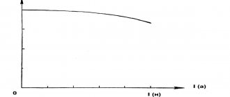
In the AD834 microcircuit, assembled in an 8-pin Cerdip (Q) package, due to the influence of parasitic inductance, the frequency response (starting at a frequency of 70 MHz) has a rise, which reaches a maximum of about 800 MHz, and then begins to decline . For other types of enclosures, the shape of the frequency response is the same, but the frequency of the beginning of the rise and the maximum of the frequency response is different. A connection in series with the input of a small damping resistor significantly reduces the peak frequency response and makes it more uniform, however, the specific value of the damping resistor depends on the topology of the printed circuit board and the chip package.
It should be noted that for the AD834, the bandwidth (bandwidth-BW) is normalized when measuring the root mean square of the input voltage without resistors in series with the input. This inclusion describes the worst operating mode, since it takes into account all factors: bandwidth, phase non-identity of channels, parasitic inductance of the housing.
The main disadvantage of PSKZ shown in Fig. 2, is the large power dissipation, which for only one AD834 multiplier is 11 mAxK4.262 V + 28 mx AK6 V = 215 mW.
In contrast to the considered PSKZ based on AD834 multipliers, the AD8361 microcircuit (Fig. 3–4) is a functionally complete mean power detector of high-frequency signals of various shapes that does not require additional active elements.
Rice. 3. Functional diagram of AD8361
Rice. 4. Typical AD8361 connection diagram
The functional diagram of the AD8361 is very close to the one shown in Fig. 2, except:
- Quadrators on multipliers with parallel-connected X- and Y-inputs are replaced by single-input quadrators, the output current of which is proportional to the square of the input voltage (transconductance cell) i = KVIv2IN.
- Instead of an emitter follower, an additional buffer amplifier with a small gain (x7.5_BUFFER) is introduced, and the DC voltage at the VRMS pin linearly depends on the RMS AC voltage at the RFIN input with a conversion factor of 7.5 V/VRMS.
- The reference voltage source (bandgap reference) has the ability to turn off the power to the microcircuit using a control signal—the “power down” mode. When a positive supply voltage is applied to the PWDN pin of the VPOS, the current consumption of the IC in the absence of an input signal decreases from 1.1 mA to
- The constant output voltage VRMS at the VRMS pin in the absence of a signal at the RFIN input VRFIN = 0 can be set by different connections of the IREF (internal reference) and SREF (supply reference) pins: VRMS = 0 if IREF is connected to VPOS, SREF connected to zero potential (Ground Referenced Mode); VRMS ≈ 350 mV, if IREF is “broken”, SREF is connected to zero potential (Internal Referenced Mode); VRMS = VPOS/7.5 if IREF and SREF are connected to VPOS (Supply Referenced Mode).
- There is a low-pass filter capacitor inside the IC (INTERNAL_FILTER), but the averaging time can be increased by connecting an external capacitor between the VPOS and FLTR pins, which reduces the voltage ripple on the VRMS pin.
Although Analog Devices indicates that the AD8361 microcircuit is operational in a wide range of frequencies, from low to 2.5 GHz, the internal structure and level of electrical parameters of the IC are designed rather for the high-frequency region. The IC supply voltage is unipolar and can range from 2.7 V to 5.5 V. This significantly reduces power consumption, but the unipolar supply voltage results in a constant voltage of ≈0.8 V at the input RFIN relative to the COMM pin. Therefore, the RFIN input can only be connected to the signal source via a coupling capacitor CC. The coupling capacitor CC, together with the matching resistor (R1 in Fig. 4) or the input resistance of the IC at the RFIN pin, equal to 225 Ohms, forms a high-pass filter (HPF), does not allow processing signals with a constant component and significantly increases low-frequency signal conversion error. A small supply voltage also does not allow increasing the linearity of the conversion of input voltage to current, as a result of which the RMS conversion error increases. Other sources of error are noise at the minimum possible signal and deviation of the quadrator transformation function from the quadratic law at the maximum.
For the AD8361, the error at 100 MHz is ≈3% over a 14 dB input signal range, which is clearly insufficient for metrology applications.
The dynamic range (DR) at the input of the microcircuit is limited by the supply voltage and the selected conversion ratio. The AD8361's output swing is a few millivolts above the zero voltage and about 100 mV below the VPOS supply voltage, so at VPOS = 5 V the maximum allowable input voltage is vINPMAX = 4.9 V / 7.5 = 653 mVrms.
In the upgraded AD8362 chip, compared to the AD8361, the input dynamic range is significantly expanded (up to 60 dB), but the remaining disadvantages of the AD8361 remain.
IC AD8362, the functional diagram of which is shown in Fig. 5, consists of:
Rice. 5. Functional diagram of AD8362
- A wideband variable gain amplifier (VGA), the gain of which GSET can be set using a special interface (setpoint interface) in the range from –21 to +39 dB depending on the voltage at the VSET pin:
where G0 is a fixed gain at VSET = 0, VGNS is a scaling voltage that determines the slope of the dependence of GSET on the control voltage VSET.
In this case, the output voltage vSIG of the VGA amplifier will be equal to
where vIN is the AC input voltage of the AD8362, which can be applied to the INHI pin when INLO is grounded, or between the INHI and INLO pins.
The VGA amplifier has an offset voltage compensation circuit (offset NULLing), which makes the amplifier's frequency response similar to a high pass filter (high pass filter) with a cutoff frequency in the low frequency region fHP. The cutoff frequency fHP should be significantly less than the operating frequency. Its value is determined by a capacitor connected to the CHPF pin:
- A reference voltage source (bandgap reference), which sets the operating mode of all IC blocks and has a VREF output with a voltage of VREF = 1.25 V.
- An attenuator with a gain of 0.06 and inputs VTGT and ACOM, the voltage VTGT between which sets the amplitude target for the voltage VSIG. If VTGT is connected to VREF and ACOM is grounded, then the voltage at the attenuator output VATG = 0.06 x 1.25 V = 75 mV.
- Two match wide-band squares with an output current proportional to the square of the input voltage
Unlike Fig. 3, in which the comparison of quadrator signals is carried out by converting their output currents into the differential input voltage of the error amplifier, in the AD8362 quadrators have different output current directions: the iSQU current is leaking, and the iTGT is sinking. When the quadrator outputs are directly connected, the difference output current will flow through the internal filter capacitor CF and the external capacitor CLPF connected between the CLPF and ACOM pins. The CLPF capacitor determines the cutoff frequency in the high frequency region of the LPF (low pass filter) fLP. Recommended value for measurement mode (Fig. 6) CLPF = 300 pF, and for work in the low-frequency region
- A non-inverting output filter amplifier (OUTPUT_FILTER), the output of which is connected to the VOUT pin, and internal resistors set buffer gain to 5.
Obviously, the internal structure of the AD8362 is quite versatile and allows for the implementation of various functions, so we will only consider enabling the IC for AC voltage measurement mode, as shown in Fig. 6.
Rice. 6. AD8362 circuit diagram for AC voltage measurement
The INHI, INLO inputs of the AD8362 microcircuit have a constant offset of ≈3.6 V relative to the ACOM pin and an input resistance of ≈100 Ohms, so their direct connection to the signal source is unacceptable and the use of coupling capacitors CCPL is required. In addition, it is recommended to connect CDECL capacitors to the decoupling terminals of the DECL chip.
In AC voltage mode, the DC current iTGT is determined by connecting the VTGT and VREF pins, and the gain GSET is determined by the voltage VOUT applied to the VSET pin. Capacitors CF and CLPF are charged by alternating current iSQU and constant iTGT to voltage VCF, which is amplified by 5 times, supplied to the VOUT, VSET pin and controls the gain of GSET. If the charge of capacitors CF and CLPF by the current iSQU is greater than the discharge by the current iTGT, then the voltage VCF and VOUT increases and, as follows from (5), GSET decreases and reduces iSQU. Such negative feedback leads to the following operating mode being established:
Avg(iSQU) = iTGT (11)
If quadrators have the same conversion coefficient, then
Avg(v2SIG) = V2ATG (12)
or taking into account (6)
where VZ =VATG/G0 is the RMS input voltage at which VSET should be equal to zero when dependence (14) is satisfied, that is, VSET =0 at
For AC voltage measurement mode, VSET = VOUT. Taking this into account and replacing the natural logarithm in (14) with a decimal one, we obtain:
where VSLP = VGNS x KLn(10) = 2.303 x VGNS is the conversion factor, that is, the change in the output DC voltage when the RMS input AC voltage changes per decade (10 times or 20 dB). For the AD8362, laser trimming of resistances on the plate is set for a frequency of 100 MHz to change the output voltage by 1 V when the RMS input voltage changes by a factor of 10 (1 V/20 dB or 50 mV/dB), and also sets VZ = 316 μV.
Direct comparison of PSKZ on AD834, AD8361, AD8362 microcircuits is difficult, since the parameters of PSKZ are not standardized by the IC manufacturer, but depend on the specific implementation of PSKZ by the consumer: topology and quality of the printed circuit board, selected types and ratings of external elements, coordination with source of the input signal, etc. The table shows only the main characteristics of the AD834, AD8361, AD8362 microcircuits, which determine the PSKZ parameters.
Table. Main characteristics of microcircuits based on analog multipliers
general information
A converter is an electrical device capable of converting electricity with some parameters into electricity with other parameters.
The following parameters are considered: current, voltage, phase.
Converters are classified into:
- controlled and uncontrolled, that is, the output parameters are either regulated or not
- electric machine (rotating) and semiconductor (static), which can be diode, thyristor and transistor
- rectifier, inverter, frequency converter, AC or DC voltage regulator, phase converter
The most common converter model today is a semiconductor thyristor or transistor converter. This is due to a number of advantages and functionality, such as: high speed and efficiency, long service life, ease of maintenance and use.
Such converters also have a number of disadvantages. For example, they are sensitive to current and voltage overloads.
Device structure
Voltage converters cannot do without the following components:
- key switching element
- power supply
- inductive power storage
- filter capacitor
- blocking diode
Depending on the order of inclusion and combination of each of the above elements, an inverting converter is created, either boost or step-down.
Principle of operation
Voltage converters (inverters), providing the maximum value of efficiency, generate voltage, the value of which is necessary to power a certain type of equipment. The transformer acts as an intermediate element that temporarily converts the voltage from a constant value to an alternating value.